Applied Materials

2.9K posts

Applied Materials banner
Applied Materials

Applied Materials

@Applied4Tech

We deliver material innovation that changes the world.

Santa Clara, California Beigetreten Ağustos 2009
1.5K Folgt16.2K Follower
Applied Materials
Applied Materials@Applied4Tech·
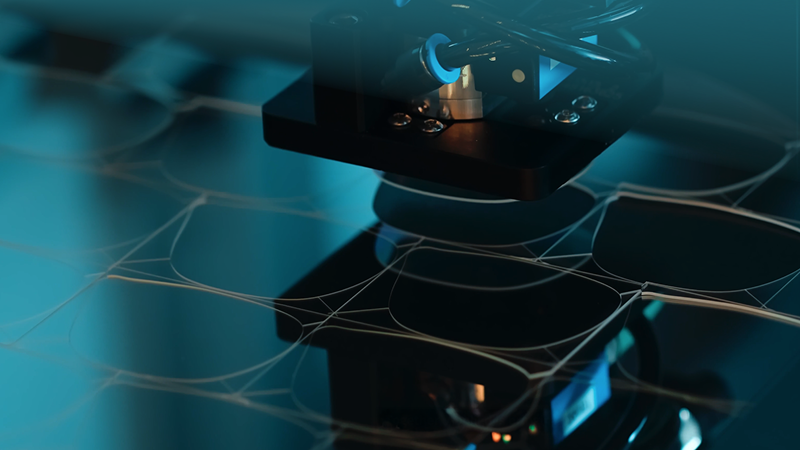
Momentum in the AR glasses market is accelerating rapidly, with waveguide-based devices growing an impressive 600% year-over-year. But with this growth comes a key challenge: delivering exceptional visual quality while ensuring AR experiences are seamless, comfortable, and truly wearable. Applied Materials is helping solve this challenge by bringing decades of materials engineering expertise and semiconductor-scale manufacturing to the AR ecosystem. Learn more: bit.ly/3QAgfXU
Applied Materials tweet media
English
1
2
18
3.9K
Applied Materials
Applied Materials@Applied4Tech·
Applied Materials has announced the expansion of our manufacturing and R&D operations in Singapore with the opening of our new Tampines Campus. This investment is designed to support the global build-out of AI infrastructure and strengthen the company’s global manufacturing footprint, which also includes facilities in the United States, Europe, Israel and Taiwan. Learn more: bit.ly/4ohktjs
Applied Materials tweet media
English
0
5
24
2.2K
Applied Materials
Applied Materials@Applied4Tech·
Applied Materials President and CEO Gary Dickerson recently joined CNBC’s Mad Money with Jim Cramer to discuss one of the most powerful shifts shaping our industry today: the rapid acceleration of AI. Dickerson's message was clear, this is a defining moment for semiconductors, stating “It is the greatest time in the history of the industry and for Applied Materials… AI is driving incredible computing demand.” As AI adoption scales across industries, the need for more powerful, energy-efficient chips continues to grow. This is driving a new wave of investment in semiconductor manufacturing and the infrastructure required to support it. With deep collaboration across our ecosystem and continued investments in innovation and capacity, Applied Materials is well positioned to help enable this transformation. Read more and watch the full interview: bit.ly/43fg8DV
Applied Materials tweet media
English
2
0
7
718
Applied Materials
Applied Materials@Applied4Tech·
Today Applied Materials announced that SCREEN Semiconductor Solutions Co., Ltd. has joined the EPIC Center as its newest innovation partner. The collaboration will bring together SCREEN SPE’s expertise in wafer cleaning technology with Applied's leadership in materials engineering to develop co-optimized process solutions for the world’s most advanced chips. “The EPIC Center is designed to dramatically accelerate the commercialization of next-generation semiconductor technologies by co-locating and co-innovating with customers and partners across the entire semiconductor ecosystem,” said Dr. Prabu Raja, President of the Semiconductor Products Group at Applied Materials. “SCREEN SPE’s wet etch and surface preparation capabilities are deeply intertwined with virtually every process step in chip manufacturing. By bringing our technologies together at the EPIC Center, we can develop co-optimized process solutions that address the increasingly complex surface engineering challenges our customers face as they push to the next technology frontier.” Learn more: bit.ly/4nQH5Hv
Applied Materials tweet media
English
9
9
44
5.3K
Applied Materials
Applied Materials@Applied4Tech·
Today Applied Materials announced that Broadcom will join Applied’s EPIC platform as an innovation partner to accelerate development of advanced chip packaging technologies critical to next-generation AI systems. “The EPIC platform is designed to drive co-innovation across the ecosystem to change the way semiconductor technologies are developed and commercialized,” said Gary Dickerson, President and CEO of Applied Materials. “This new model gives leading system designers like Broadcom early access to foundational innovations in materials and process equipment, providing an opportunity for deep collaboration to accelerate the introduction of new advanced packaging technologies.” Learn More: bit.ly/4nD1rDY
Applied Materials tweet media
English
2
2
20
1.8K
Applied Materials
Applied Materials@Applied4Tech·
Our Q2 FY26 financial results included record revenue and earnings, along with our highest gross margin in more than 25 years. Applied's strong momentum is driven by rapid global AI infrastructure expansion, leadership in key high-value semiconductor markets, and our agile operations and supply chain execution to meet rising demand. Learn more: bit.ly/43an6d9
Applied Materials tweet media
English
0
0
14
786
Applied Materials
Applied Materials@Applied4Tech·
Applied Materials has announced that @ASU, @rpi and @StanfordEng will join the company’s EPIC Center in Silicon Valley as inaugural research partners. Through close collaboration with Applied’s scientists and engineers, university teams will engage in high velocity research programs across advanced materials, novel process and device technologies, and chip architecture inflections – leveraging the synergy of academia and industry to accelerate energy efficient innovations for next generation AI chips. ir.appliedmaterials.com/news-releases/…
Applied Materials tweet media
English
3
3
12
1.4K
Applied Materials
Applied Materials@Applied4Tech·
Today Applied Materials announced a new innovation partnership with TSMC to accelerate the development and commercialization of semiconductor technologies required for the next era of AI. Working together at Applied’s EPIC Center in Silicon Valley, the companies will co-innovate to advance materials engineering, equipment innovation, and process integration technologies designed to deliver energy-efficient performance from the data center to the edge. “Applied and TSMC share a long history of deep collaboration built on trust and a shared commitment to advancing innovation at the leading edge of semiconductor technology,” said Gary Dickerson, President and CEO of Applied Materials. “By bringing our teams together at the EPIC Center, we are strengthening that partnership and accelerating the development of technologies to address the unprecedented complexity driving the chipmaking roadmap.” Learn more: bit.ly/3Ryr9xj
Applied Materials tweet media
English
4
7
33
2.6K
Applied Materials
Applied Materials@Applied4Tech·
Today we announced we have entered into a definitive agreement with ASMPT SEMI Solutions to acquire its ASMPT NEXX, Inc. business, a leading supplier of large-area advanced packaging deposition equipment for the semiconductor industry. The addition of the NEXX team and products will broaden Applied’s portfolio of panel-level advanced packaging technologies which are designed to enable chipmakers and systems companies to build larger-body AI accelerators for higher energy-efficient performance. Learn more: bit.ly/3P7fcxM
Applied Materials tweet media
English
7
15
106
21.5K
Applied Materials
Applied Materials@Applied4Tech·
As AI drives demand for faster, more energy‑efficient chips, transistor customization is becoming just as important as scaling. The Applied Materials Trillium™ system enables chipmakers to precisely engineer materials at the atomic level, allowing transistor performance to be tuned for specific AI workloads. By combining advanced deposition, integration and process control in a single platform, Trillium helps speed development of next‑generation devices while delivering better power, performance and yield at leading‑edge nodes - a key step toward more flexible, application‑optimized semiconductors in the AI era. Learn more: bit.ly/4tu72id #MakeItMaterial
Applied Materials tweet media
English
5
7
42
2.8K
Applied Materials
Applied Materials@Applied4Tech·
Want to learn more about Applied's material innovation in transistors but missed our recent Leading the Future of Logic Master Class? Watch this video where we describe how shallow trench isolation enables increased transistor speed and power efficiency. #MakeItMaterial
English
4
2
10
1.4K
Applied Materials
Applied Materials@Applied4Tech·
Today we announced that Advantest Corporation, a leading semiconductor test equipment supplier, will join Applied’s EPIC platform as an innovation partner to strengthen the links between front-end manufacturing technologies and back-end testing of chips and packages, helping chipmakers bring new designs to market faster. To support this partnership, Advantest has established a new, state-of-the-art Innovation Center on Applied Materials’ R&D campus in Silicon Valley, that will seamlessly connect with Applied’s EPIC Center. “Applied Materials designed the EPIC platform to dramatically accelerate the commercialization of next-generation semiconductors by co-locating and co-innovating with our customers and partners,” said Gary Dickerson, President and CEO of Applied Materials. “By collaborating side-by-side with Advantest, we can develop solutions that enable chipmakers to optimize end-to-end semiconductor production flows and bring new designs to market faster and more efficiently.” Learn more about the partnership: ir.appliedmaterials.com/news-releases/…
Applied Materials tweet media
English
1
2
16
845
Applied Materials
Applied Materials@Applied4Tech·
AI is driving the semiconductor industry into the angstrom era. Next‑generation AI GPUs in development are expected to integrate 300+ billion transistors on a single chip, pushing performance, power efficiency, and manufacturability to new limits. Applied Materials’ Producer™ Precision™ Selective Nitride PECVD system addresses one of the toughest challenges in advanced GAA logic: preserving shallow trench isolation (STI) at atomic‑scale dimensions. Using an industry‑first selective bottom‑up deposition, the system places dense silicon nitride only where needed, protecting isolation through 500+ downstream process steps. The result: lower parasitic capacitance, reduced leakage, and improved performance‑per‑watt without damaging sensitive underlayers - all thanks to low‑temperature processing. Now being adopted by leading foundry‑logic manufacturers at 2nm and beyond, Precision Selective Nitride highlights how materials engineering, not lithography alone, is driving the next phase of chip scaling. Learn more: bit.ly/4cf85Lx #Semiconductors #AIHardware #AdvancedLogic #GAA #2nm #ChipManufacturing #AppliedMaterials #ProcessTechnology
Applied Materials tweet media
English
1
2
15
843
Applied Materials
Applied Materials@Applied4Tech·
We’re excited to introduce two new deposition systems designed to meet the extreme complexity of Gate-All-Around (GAA) architectures: 🔹Precision™ Selective Nitride PECVD 🔹Trillium™ ALD Together, these systems give leading logic manufacturers the materials precision needed to deliver faster, more power‑efficient chips at the most advanced nodes. Learn more: bit.ly/4cf85Lx
Applied Materials tweet media
English
2
8
42
4.3K
Applied Materials
Applied Materials@Applied4Tech·
Welcome back to Applied’s semiconductor chip city where we talk about each piece of the city works together to make a real, meaningful difference. Imagine multilayer metal highways connecting every part of a chip. That’s our focus for today: interconnects. 🛣️ Interconnects route signals across and between layers of metal at lightning speed. These interconnects are like a highway of innovation within our semiconductor chip city. Learn more about our Interconnect solutions: bit.ly/3NWEAG5 We deliver material innovation that changes the world. #MakeItMaterial
English
1
1
8
669
Applied Materials
Applied Materials@Applied4Tech·
Applied Materials is proud to announce a long-term collaboration agreement with @SKhynix to accelerate the development and deployment of next-generation DRAM and high-bandwidth memory (HBM). Engineers from both companies will work side-by-side at Applied’s EPIC Center in Silicon Valley to advance innovation in materials, process integration and 3D advanced packaging as memory architectures move beyond current production nodes. President and CEO Gary Dickerson shared, “Applied Materials and SK hynix share a long history of working together to improve the energy-efficient performance of advanced memory chips through innovations in materials engineering,” He added, “We are excited to have SK hynix join the EPIC Center as a founding partner, and we look forward to driving further breakthroughs together that accelerate commercialization of next-generation DRAM and HBM technologies for the AI era.” Learn more: bit.ly/4rpcuB0
Applied Materials tweet media
English
1
11
81
15.5K
Applied Materials
Applied Materials@Applied4Tech·
We're excited to announce we are working with Micron Technology to develop next-generation DRAM, high-bandwidth memory (HBM) and NAND solutions that increase the energy-efficient performance of AI systems, bringing together advanced R&D capabilities from our EPIC Center in Silicon Valley and Micron’s state-of-the-art innovation center in Boise, Idaho to strengthen the semiconductor innovation pipeline in the United States. Here’s what our CEO, Gary Dickerson, had to say: “Applied Materials and Micron have a long-standing partnership focused on driving higher performance and more energy-efficient advanced memory chips by pushing the boundaries of materials engineering and manufacturing innovation,” said Gary Dickerson, President and CEO of Applied Materials. “We are excited to deepen our collaboration with Micron as a founding partner at the EPIC Center as next-generation memory technologies play an increasingly vital role in the future of AI systems.” Learn more: bit.ly/4byPdrs
Applied Materials tweet media
English
0
9
78
12.9K
Applied Materials
Applied Materials@Applied4Tech·
Pushing AI performance requires increasingly tighter tolerances and extreme precision. Applied's Sym3™ Z Magnum™ conductor etch system extends the proven Sym3 Z platform by bringing plasma and ion control closer to the wafer, delivering angstrom‑level etch control, improving wafer uniformity and enabling faster, more energy‑efficient chips. bit.ly/4kZMKJN
Applied Materials tweet media
English
0
5
22
1K
Applied Materials
Applied Materials@Applied4Tech·
Inside every chip, there’s a tiny metal contact, or bridge, that helps electricity move between layers. As chips get smaller and AI demands more speed, these tiny contacts have become a major bottleneck. Applied Materials is enabling the next generation of contact scaling using molybdenum, a material that keeps electricity flowing faster, even at the most advanced nodes. Learn more about our materials engineering expertise: bit.ly/4rsMs0y
Applied Materials tweet media
English
3
4
15
791