Atomiclayerdeposition.com retweetledi
Atomiclayerdeposition.com
204 posts

Atomiclayerdeposition.com
@aldjournal
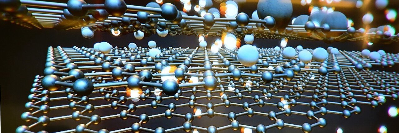
Diamond open access journal “Atomic Layer Deposition, International Journal” and interactive ALD news and community website #aldep
Amsterdam, Netherlands Katılım Ekim 2021
1K Takip Edilen449 Takipçiler

Atomiclayerdeposition.com retweetledi

Thank you for your incredible support this year! From all of us at Kurt J. Lesker Company, we wish you a joyful holiday season filled with peace, happiness, and success. Merry Christmas & Happy Holidays!
#MerryChristmas #HappyHolidays #VacuumTechnology
English
Atomiclayerdeposition.com retweetledi
This holiday season, our Jefferson Hills team is proud to continue a tradition that’s close to our hearts. Once again, we’re supporting the Family Foundations Early Head Start Angel Tree program.
#KurtJLesker #GivingBack #CommunityImpact #TeamLesker


English
Atomiclayerdeposition.com retweetledi
As the AR market rapidly expands, manufacturers face the challenge of combining optical quality with scalable production. Discover our latest Insight to see how Beneq’s C2R™ is enabling the shift from lab-scale to volume production: hubs.li/Q03YBC4Y0
#ALDep
English
Atomiclayerdeposition.com retweetledi
Bringing supercapacitor innovations from research to production requires early focus on scalability. In the ARMS program, Beneq helps bridge the gap by turning validated ALD processes into stable, production-ready solutions for industry. Learn more: hubs.ly/Q03YrWcq0
#ALDep
English
Atomiclayerdeposition.com retweetledi
Ready to apply your mechanical design expertise to next-generation ALD hardware? Join Beneq as a Mechanical Engineer in our Advanced ALD Business Unit, P-Series Team. Apply by January 6, 2026. For more info: hubs.li/Q03XYtQ10
#ALDep
English
Atomiclayerdeposition.com retweetledi
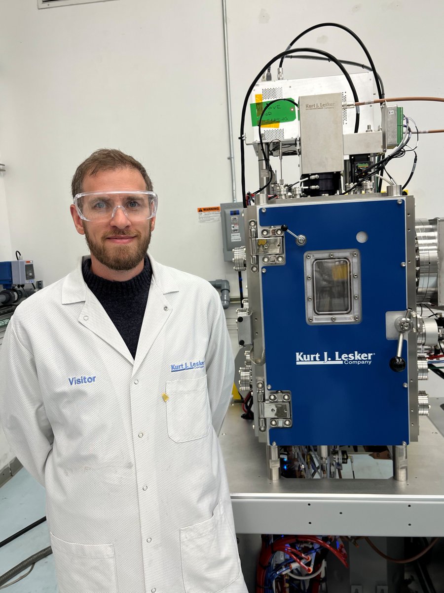
Proud to complete FAT on a PVD75 sputtering system for @oistedu!
Great working with Stéphan onsite. This tool will power diverse thin-film applications in OIST’s multi-user facility. Excited to support this innovative community!
#PVD75 #Sputtering #ThinFilmDeposition #KJLC
English
Atomiclayerdeposition.com retweetledi
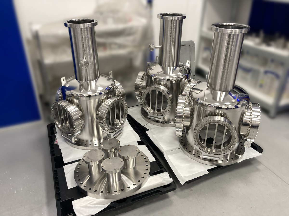
Chimneys for @Princeton’s DarkSide20k experiment at Gran Sasso are ready to ship. They’ll provide contamination-free paths for cables & fibers to the DAQ. Huge thanks to Andrea Ianni & our team for precision craftsmanship.
#DarkSide20k #DarkMatterResearch #KJLC
English
Atomiclayerdeposition.com retweetledi
Finland’s semiconductor field is scaling fast – but growth depends on the next generation of talent. Beneq has joined eight other companies to launch Chips Finland, campaign to promote career paths in the sector. Follow @chipsfinland on Instagram.
#ALDep

English
Atomiclayerdeposition.com retweetledi
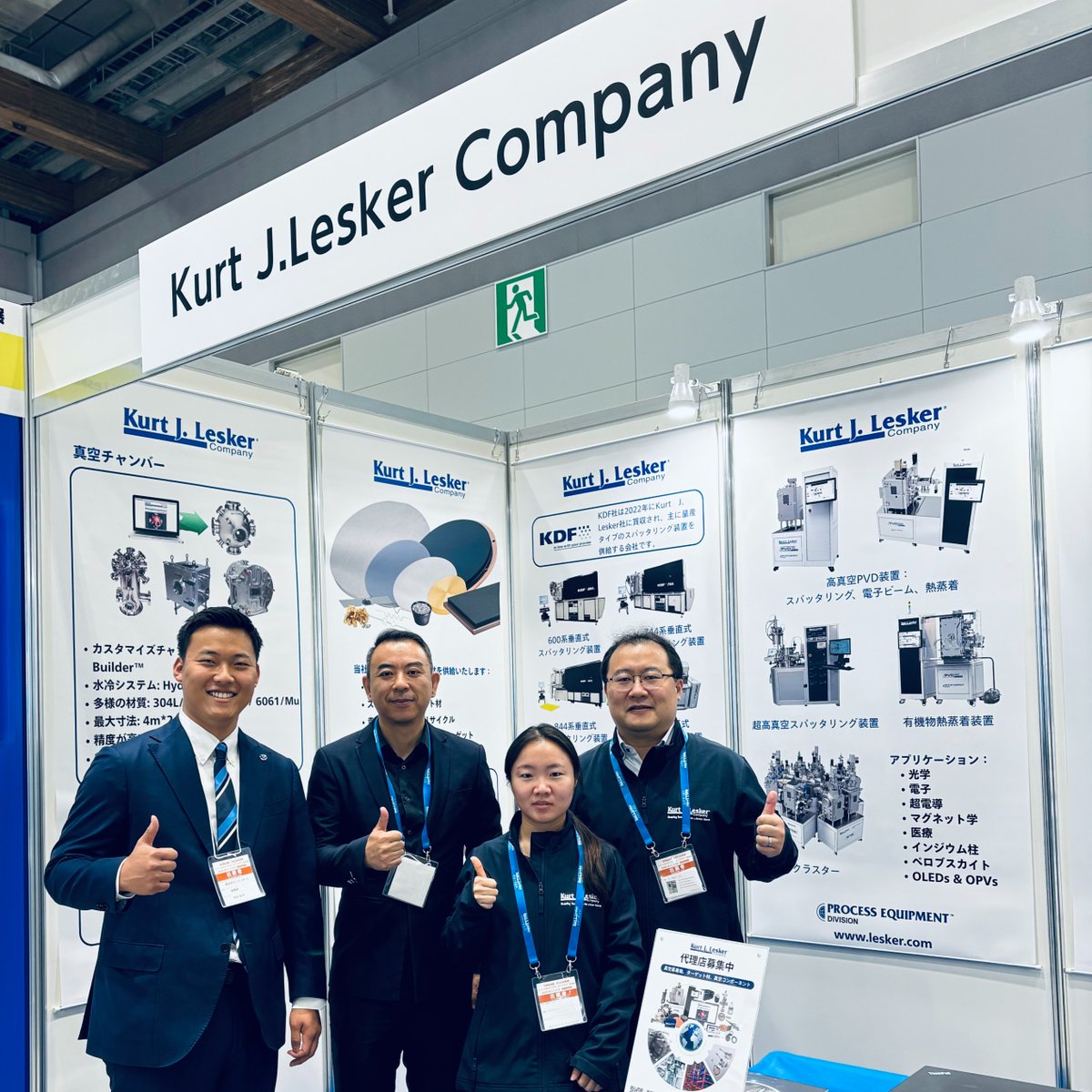
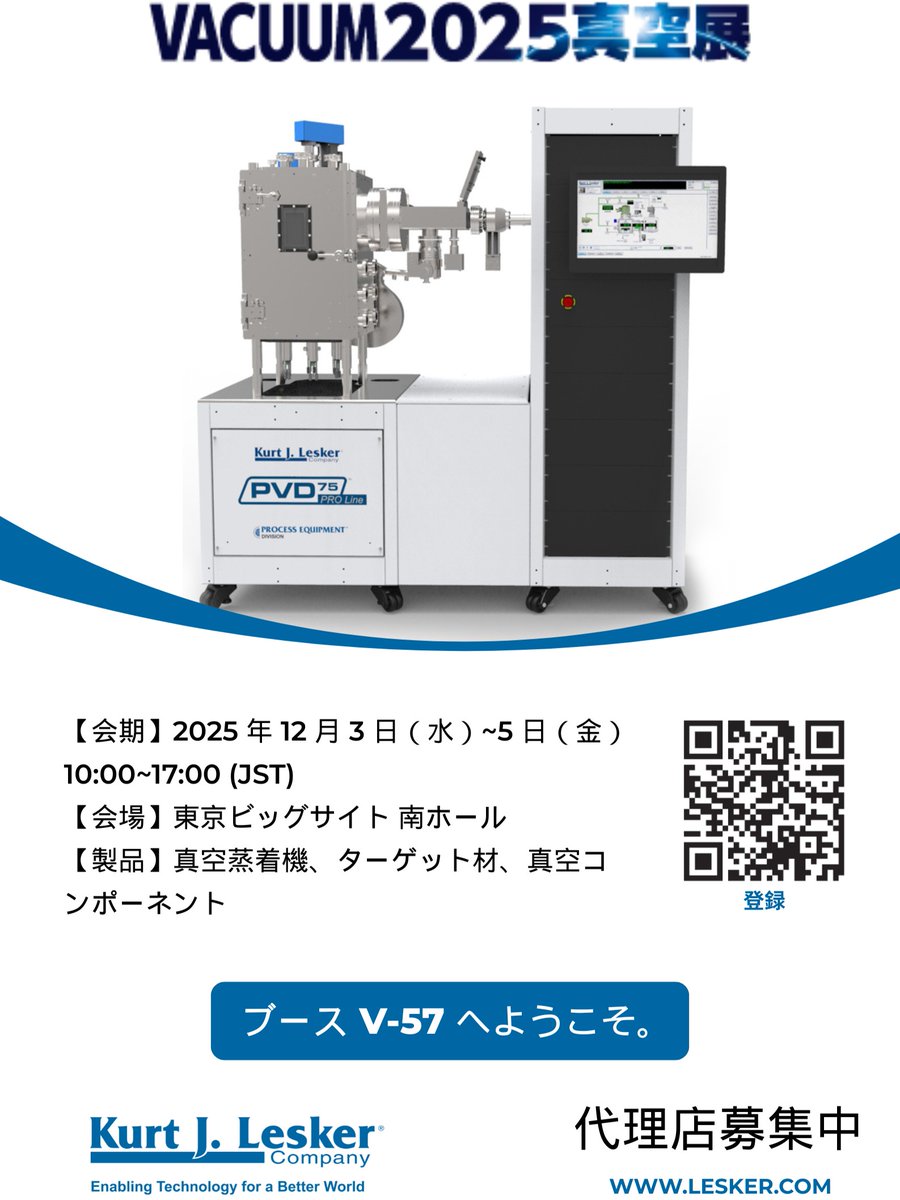
KJLC at VACUUM 2025! Meet Aaron (Chinese/Japanese/English) for 1:1 talks on products & vacuum solutions. Booth V-57, Tokyo Big Sight, Dec 3–5, 10:00–17:00. Eager to connect with traders & agencies.
biz.nikkan.co.jp/eve/vacuum/en/
#VACUUM2025 #KJLC #真空技術 #半導体 #先端材料 #東京展示会
English
Atomiclayerdeposition.com retweetledi
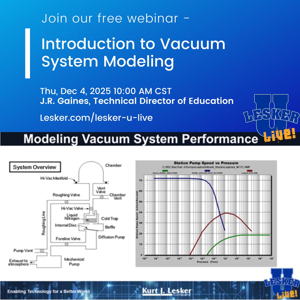
Free webinar: Introduction to Vacuum System Modeling
Date: Dec 4, 2025, 10:00 AM CST
Speaker: J.R. Gaines, Technical Director of Education
forms.office.com/pages/response…
#VacuumTechnology #AdvancedManufacturing #VacuumSystem #FreeWebinar #EnablingTechnologyForABetterWorld
English
Atomiclayerdeposition.com retweetledi
Join us at @mit_nano for an ALD Tech Talk with Kurt J. Lesker experts!
Explore UHP conditions for low-oxygen nitride films via PEALD, key for next-gen semiconductors.
Ultra-High Purity Conditions in ALD
Dec 10, 2025, 11:00-13:00 ET
mitnano.mit.edu/events/tool-ta…
#ALD #PEALD #MITnano

English
Atomiclayerdeposition.com retweetledi
On November 25, join SEMI and Beneq for a webinar with Dr. Alexander Perros on how ALD is reshaping protective coatings for advanced-node manufacturing. Secure your spot here: hubs.li/Q03VDfKT0
#ALDep
English
Atomiclayerdeposition.com retweetledi
We are excited to introduce Beneq Transform® XP – a second-generation ALD platform for Wide Bandgap power and RF devices. It combines advanced PEALD tuning, in-cycle annealing, and breakthrough throughput in a scalable, production-ready system: hubs.li/Q03VC9N90
#ALDep
English
Atomiclayerdeposition.com retweetledi
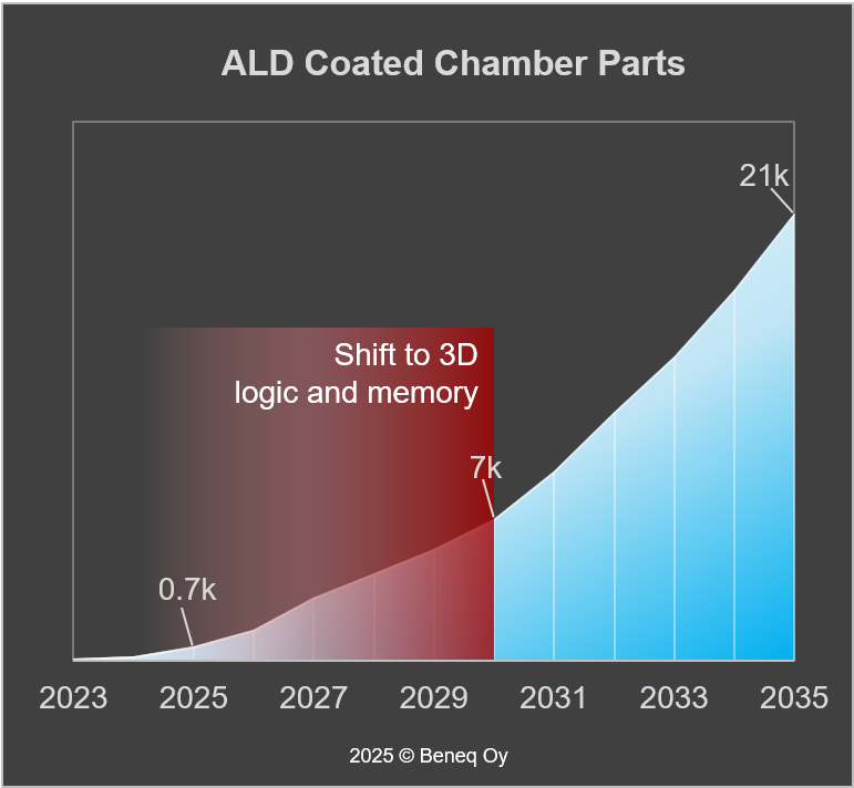
Beneq projects ALD-coated chamber part demand to surge to 21,000 units by 2035. Discover the opportunity with SEMI and Beneq. Register: hubs.li/Q03Vbtwp0
#ALDep
English
Atomiclayerdeposition.com retweetledi
We are excited to announce Beneq Transmute™, our next-generation ALD platform designed for high-volume production of Wide Bandgap (WBG) power devices, advanced RF components, μLEDs, and other specialty semiconductor applications. Read more: hubs.li/Q03TZSjR0
#ALDep
English
Atomiclayerdeposition.com retweetledi
Excited to share: our ALD-150LX system is now fully installed at @argonne, supporting the Guha Group’s cutting-edge research in microelectronics & quantum science. Proud to enable innovation with @uchicago!
#ALD #Nanotechnology #QuantumResearch #Innovation

English
Atomiclayerdeposition.com retweetledi
Free Webinar: Introduction to Plasma Emission Monitoring
Date: Thursday, 13 November 2025
Time: 11:00 AM EDT
Speaker: Nick Franzer
forms.office.com/r/dWNPPneS09
#ThinFilm #PlasmaEmissionMonitoring #PVD #HiPIMS #AdvancedMaterials #LeskerULive #enablingtechnologyforabetterworld

English
Atomiclayerdeposition.com retweetledi
Beneq will be exhibiting at SEMICON Europa 2025, taking place 18-21 November in Munich. Visit us at the ICM Foyer, booth #6, next to the Fab Management Forum, on November 19-20: hubs.li/Q03RNChC0
#ALDep #SEMICONEuropa #SEMICON
#Microelectronics
English
Atomiclayerdeposition.com retweetledi
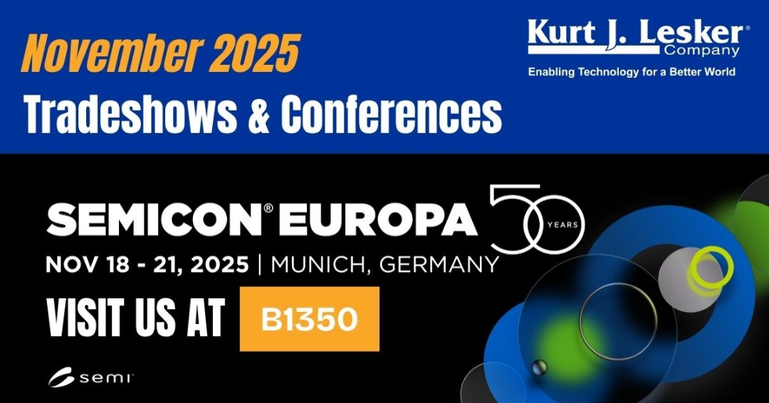
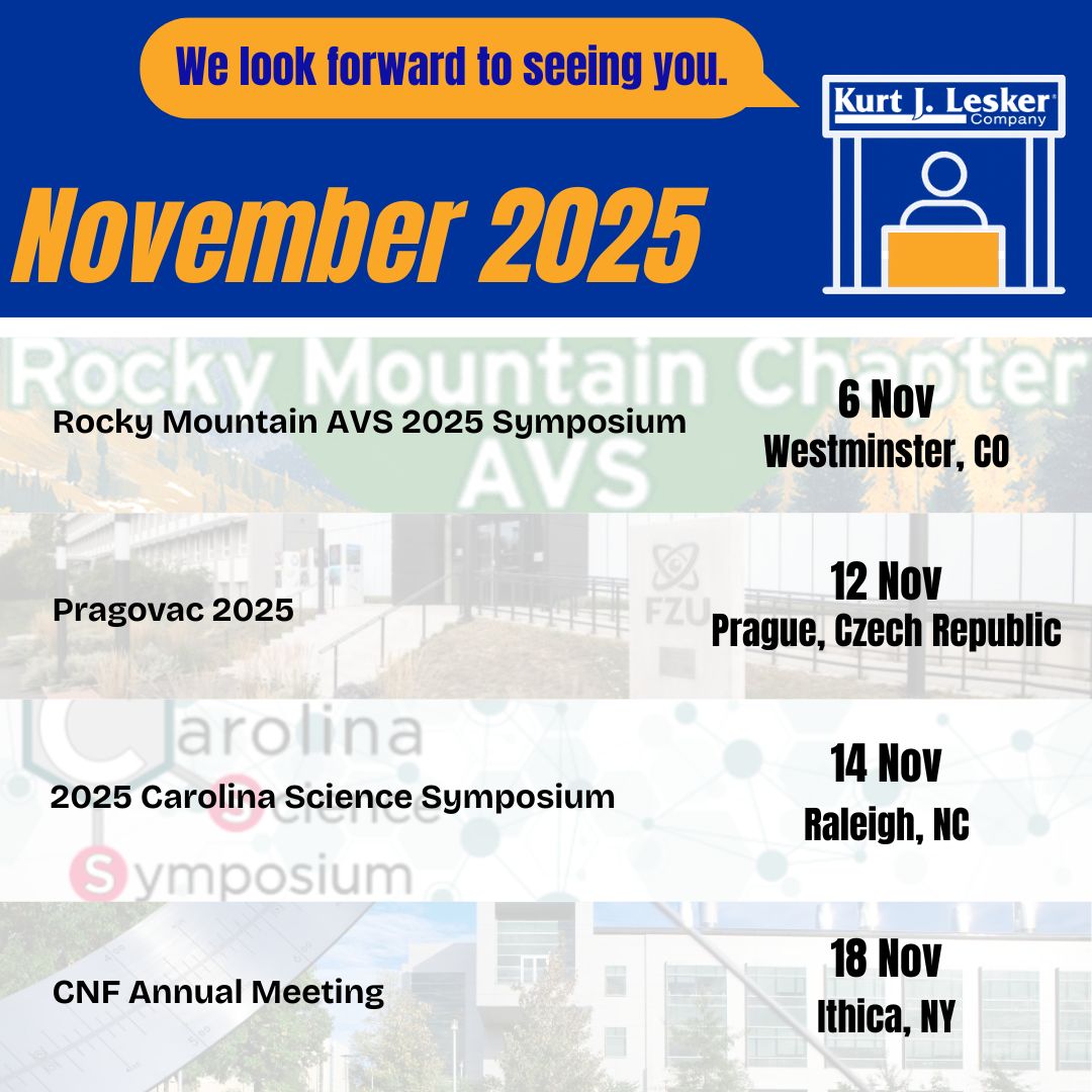
Our November event lineup is here -
🔹Nov 6 Rocky Mountain AVS (CO)
🔹Nov 12 Pragovac (Prague)
🔹Nov 14 Carolina Science Symposium (NC)
🔹Nov 18 CFN Annual Meeting (NY)
🔹Nov 18–21 SEMICON Europa (Munich, Booth B1350)
#NovemberExhibition #VacuumTechnology #Exhibitions2025
English