Longoria

9.7K posts

Longoria

Longoria

@ElliotL45

Sumali Şubat 2015
1.4K Sinusundan225 Mga Tagasunod
Longoria nag-retweet
Out Of Context OM
Out Of Context OM@oContextOM·
c'est legendaire, mythique, historique, les mots me manquent pour exprimer à quel point cette interview rentrera de gré ou de force dans l'Histoire du club avec un grand H
Français
272
1.4K
9.9K
607.6K
Longoria nag-retweet
BeFootball
BeFootball@_BeFootball·
COMMENT NE PAS CHIALER 😭 : 𝗚𝗥𝗜𝗘𝗭𝗠𝗔𝗡𝗡 🇫🇷 𝗦𝗘 𝗙𝗔𝗜𝗧 𝗙𝗘́𝗟𝗜𝗖𝗜𝗧𝗘𝗥 𝗣𝗔𝗥 𝗟’𝗨𝗡𝗘 𝗗𝗘 𝗦𝗘𝗦 𝗜𝗗𝗢𝗟𝗘𝗦 𝗧𝗛𝗜𝗘𝗥𝗥𝗬 𝗛𝗘𝗡𝗥𝗬. 🐐❤️ « MERCI POUR TOUT CE QUE T’AS FAIS DANS LE FOOT. POUR LES BLEUS. POUR LE FOOT FRANÇAIS. » WOW.
Français
30
1.7K
28.2K
591.7K
Longoria
Longoria@ElliotL45·
@jukan05 Well I hope it does. I bought $GOOGL at that time and I just bought $MSFT
English
0
0
0
184
Jukan
Jukan@jukan05·
I respect the people who bought $GOOGL when Bard came out and everyone thought Google was sinking. It feels just like buying $MSFT right now, doesn’t it?
English
70
18
700
120.8K
Longoria
Longoria@ElliotL45·
@BourseAsieFR Il y a qques tu disais que le yield était horrible et que les coûts pouvaient exploser pour Intel, c'est tjrs le cas ?
Français
1
0
0
743
BourseAsieFR
BourseAsieFR@BourseAsieFR·
🚨 Google est peut-être en train de retirer un contrat à TSMC. Selon les analystes d'Aletheia (janvier 2026), le prochain TPU de Google (2nm, nom de code HumuFish) adopterait un format de puce extrême 9 à 10 fois la taille d'une puce standard. Ce n'est pas confirmé officiellement, mais c'est ce que surveille Morgan Stanley. Le problème : à cette taille, l'encapsulation devient un casse-tête industriel. TSMC peut techniquement le faire avec sa technologie CoWoS-L. Mais Intel propose une approche alternative (EMIB) pour ce type de format géant. TSMC reste le seul à pouvoir graver les puces 2nm de Google. La compétition Intel/TSMC porte sur le "backend", pas sur la puce elle-même. Où en est Intel ? EMIB-T, leur version pour très grands formats IA, entre en production en 2026 mais sans client commercial confirmé à ce stade. Les premiers designs Google en EMIB standard sont attendus pour 2027/2028 (TPU v9). Ce que ça change pour les investisseurs : $TSM reste intouchable sur la fabrication. Mais sur l'encapsulation de formats extrêmes, la domination n'est plus acquise d'avance. Intel joue une carte réelle pas encore gagnante, mais crédible à horizon 2028.
BourseAsieFR tweet media
Français
7
16
166
32K
M8 Shun ⭐️
M8 Shun ⭐️@M8_Shun·
Si vous me connaissez ou que vous me suivez un peu, vous savez que j’aime faire la fête avec les copains. Mais après ce week-end… difficile de ne pas changer d’avis. À 10h du matin, ils servent déjà des doubles pintes. Résultat ? Des mecs complètement ivres dès le matin, qui vomissent partout, insultent tout le monde et se prennent pour des rois… Franchement, quand on voit ça, je suis totalement pour arrêter la vente d’alcool pendant les majors. Si vous voulez boire, allez au bar après le match avec vos potes 🙏 @Gotaga @xSqueeZie @BrokyBrawks @gentlemates
M8 idriix@idriix_

Juste avant de dormir, je me permets de vous faire une petite demande les CEO, PAR PITIÉ interdisez l’alcool au Major de Paris.. Un grand nombre de gens ne savent plus se tenir à la moindre goutte d’alcool… Certain comme moi attendent le retour d’un événement CoD en France depuis plus de 10 ans quasiment et l’alcool on peut tellement tout gâcher d’une minute à l’autre.. donc pls c’est la SEULE demande que j’ai à vous faire ! Merci d’avance à vous ! 🙏🏼 @gentlemates @Gotaga @xSqueeZie @BrokyBrawks @Nikof 🩷🩷 #M8WIN #GentleMates

Français
24
43
710
154.8K
Cerfia
Cerfia@CerfiaFR·
🇫🇷💍 "T’es en train de me faire quoi là?". Un futur marié a dit NON à sa femme dans l’émission 4 Mariages pour une Lune de Miel dans un épisode "surprises aux invités".
Français
161
704
8.2K
2M
Longoria
Longoria@ElliotL45·
@YannP42 @VqZvlr @RiotGamesFrance Tu connais le jeu ? Tu y as déjà joué ? Si oui qu'est ce que tu ne comprends pas ? Si tu ne connais pas le jeu aucune raison d'etre aussi condescendant parce que son message est totalement compréhensible
Français
0
0
3
334
FL VqZ
FL VqZ@VqZvlr·
L'entretien pour bosser chez @RiotGamesFrance sur le support il faut avoir 10 d'IQ maximum impossible autrement. Même un gosse de CE1 comprend ce que je demande, j'espère sincèrement que ces gens ne sont pas payés.
FL VqZ tweet mediaFL VqZ tweet media
Français
45
36
1.7K
242.6K
Longoria
Longoria@ElliotL45·
@yamakhalah @VqZvlr @Amazigh_Chahid @RiotGamesFrance Tu joues à Valorant ? Tu connais le jeu ? Si ce n'est pas le cas normal de ne pas comprendre. Si tu connais le jeu tu as effectivement 10 de QI. Par contre les personnes qui disent c'est qui qui plutôt que qui est ce qui ont effectivement 10 de QI oui.
Français
0
0
1
74
WL Yamakhalah
WL Yamakhalah@yamakhalah·
@VqZvlr @Amazigh_Chahid @RiotGamesFrance Tu sais pas faire une demande de manière concise et concrète. On est plusieurs à te le signaler. Tu refuses d’entendre que tu pourrais être celui qui cause le problème pour lequel tu te plaint. Alors c’est qui qui a 10 de QI ? 🥲
Français
3
0
12
2.4K
Terrible Maps
Terrible Maps@TerribleMaps·
Soft drinks of Europe
Terrible Maps tweet media
English
631
386
7.7K
8.6M
Longoria
Longoria@ElliotL45·
@Kelawin130 Oui bon t'as jamais joué au foot en gros
Français
1
0
57
9.2K
Longoria
Longoria@ElliotL45·
@Frenchie_ Yes mais c'est pas nouveau que Micron a qd même de gros soucis à suivre la cadence des deux concurrents sud coréen !
Français
0
0
0
60
Frenchie
Frenchie@Frenchie_·
La mémoire est devenue l’un des goulots d’étranglement centraux de l’IA depuis fin 2025, tant en capacité qu’en bande passante, ce qui en fait un des drivers majeurs du cycle actuel des semi. Pour adresser ce mur mémoire, plusieurs solutions se dessinent (HBM3E/HBM4, CXL-pooling, architectures rack-scale), et l’on retrouve presque systématiquement Samsung, SK hynix et Micron comme fournisseurs critiques de DRAM/HBM et de modules pour data centers. Mes deux picks sont : >Astera Labs ( $ALAB ), qui fournit les contrôleurs mémoire CXL au cœur des architectures de pooling. >Micron ( $MU ), qui s’est repositionné comme leader US de la mémoire AI (HBM, DRAM data center, NAND) Deux picks “memory pur” particulièrement bien placés pour capter ce super-cycle.
Frenchie tweet media
The Kobeissi Letter@KobeissiLetter

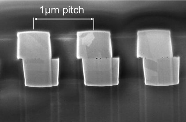
Nvidia's AI chips are consuming memory at an unprecedented pace: Nvidia's, $NVDA, most recent Rubin chip now requires 288GB of RAM. This is +800% more than the memory of a high-end PC, and +2,300% more than a high-end smartphone. By comparison, the H100, launched 4 years ago, needed 80GB of RAM, or 72% less. In other words, each new generation of Nvidia AI chips requires significantly more memory than the last, putting enormous strain on global supply. Furthermore, AI giants like Alphabet, $GOOGL, and OpenAI are locking up large portions of the global memory chip supply by purchasing millions of Nvidia AI chips. As a result, average spot prices for 16GB DDR4 RAM are up +2,352% YoY to a record $76.90, while 8GB DDR4 prices are up +1,873% YoY, to an all-time high of $28.90. The global memory chip shortage is out of control.

Français
7
4
79
8.8K
🇫🇷Yass🇵🇸
🇫🇷Yass🇵🇸@Yass69AMG·
@ChallandRomain Alors non , j’me suis fais avoir un matin sans faire attention j’avais mis de l’essence avec un prix à plus de 7€ le litre , j’avais pas fais attention c’était une erreur de saisie , j’ai dû repasser à l’accueil pour me faire rembourser la différence
Français
1
0
2
6.9K
Romain Challand
Romain Challand@ChallandRomain·
Jean-Michel, retraité, va dans quelques jours s’enchaîner à la préfecture et débuter une grève de la faim parce que Carrefour lui aura débité le montant rectifié
Focus@FocusinfosFr

🇫🇷⛽️ INCROYABLE BUG À LA POMPE ! Station Carrefour Market de Breuillet (Essonne) : le litre d’essence affiché à 0,01 € (1 centime) par erreur de saisie ! Ruée immédiate : files interminables, bidons sortis des coffres, chaos total en quelques minutes.

Français
39
375
9.1K
918.9K
Longoria
Longoria@ElliotL45·
@neverlongqcom @ContrarianCurse @IanCutress I hear you on the speeds, vendors definitely deviate to flex performance. But for packaging mechanics, physical specs are the law. You can't dual-source HBM if everyone has a different Z-height or bump pitch
English
1
0
0
78
theconductor
theconductor@neverlongqcom·
@ElliotL45 @ContrarianCurse Old as in we already had headlines around the manufacturers trying the gap narrowing (see trend force earlier in the week. Also why are the planned HBM pin speeds not at the JEDEC standard? following JEDEC is not mandatory? Would suggest you see @IanCutress recent note on this.
English
1
0
0
82
SuspendedCap
SuspendedCap@ContrarianCurse·
Oh $BESI ouch hahaha you fucker Whole market gunna get porked. Doubt my long save me this time, I was holding in nicely
English
4
0
43
9.1K
Longoria
Longoria@ElliotL45·
@neverlongqcom @ContrarianCurse Wdym it’s old? These specs are defined by the memory makers and the customers themselves. HBM is a commodity, so following JEDEC is mandatory for interoperability. Only custom HBM can afford to deviate. No spec, no scale.
English
1
0
0
106
theconductor
theconductor@neverlongqcom·
@ContrarianCurse JEDEC stuff is old, no one adheres to that anyways…don’t think this changes the hybrid bonding thesis - if anything this makes the underfill bonding process more difficult. Rip my besi bags tho
English
1
0
2
446
Longoria
Longoria@ElliotL45·
@pauluscremers @jukan05 Well, it was true, they announced a relaxation of the thickness from 720um to 775um which was true
English
0
0
0
44
Jukan
Jukan@jukan05·
Next-Gen HBM Thickness Relaxation Gains Momentum… A Blow to Hybrid Bonding Major semiconductor companies are reportedly in discussions to relax the thickness standard for next-generation high-bandwidth memory (HBM), which requires 20-layer stacking. Figures ranging from 825 to 900 micrometers (μm) and above are being floated — surpassing the 775μm thickness of HBM4 (6th-generation HBM), which is set for full commercialization this year. According to ZDNet Korea's reporting as of the 6th, participants in JEDEC (the Joint Electron Device Engineering Council) are actively discussing a significant relaxation of thickness standards for next-generation HBM. Next-Gen HBM Thickness Standard: Discussions Reach 825–900μm and Beyond HBM is a next-generation memory built by vertically stacking multiple DRAM dies and connecting them via microscopic bumps. Through HBM3E, the thickness standard had been held at 720μm, but it was raised to 775μm with HBM4, largely due to the increased stack count of 12 and 16 layers — up from 8 and 12 in the previous generation. Now, the industry is discussing further relaxation of thickness standards for next-generation HBM — namely HBM4E and HBM5 — which will stack DRAM in 20 layers. The figures currently under discussion range from 825μm to over 900μm. Should the standard be set above 900μm, the increase would substantially exceed any prior jump. "JEDEC needs to finalize key standards one to one-and-a-half years before a product reaches commercialization, so discussions around next-gen HBM thickness are very active right now," said one semiconductor industry official. "Figures above 900μm are already being thrown around." JEDEC is the international standards body for semiconductor products. Its membership includes memory companies such as Samsung Electronics, SK Hynix, and Micron, as well as major global semiconductor firms including Intel, TSMC, NVIDIA, and AMD. Historically, the industry has been extremely strict about limiting HBM thickness increases. If HBM were allowed to grow thicker without constraint, it would become increasingly difficult to match the thickness of system semiconductors — such as GPUs — that are integrated horizontally alongside it. Excessive spacing between DRAM layers also lengthens data transmission paths, degrading performance and efficiency. As a result, memory companies have pursued a range of technologies to keep HBM thin, most notably thinning processes that grind down the backside of core DRAM dies, and bonding technologies that reduce inter-die spacing. Both Memory and Foundry Players Want Thickness Relaxation Despite these efforts, there are two primary reasons why the industry is now actively discussing relaxing the thickness standard for next-generation HBM. The first is the shift to 20-layer stacking. Existing thinning processes and inter-die bonding technologies are approaching their limits in terms of how thin HBM can realistically be made. The packaging roadmap of TSMC, a leading foundry, is also a contributing factor. TSMC currently holds a near-monopoly on 2.5D packaging (CoWoS), which integrates HBM and GPUs into a single AI accelerator. CoWoS uses a wide interposer inserted between the chip and substrate to enhance packaging performance. TSMC's next step beyond 2.5D packaging is SoIC (System-on-Integrated Chips), which vertically stacks system semiconductors at extremely fine pitch in a true 3D configuration. In AI accelerator applications, TSMC-SoIC would combine the stacked system semiconductor with HBM. When TSMC-SoIC is applied, the thickness of the system semiconductor increases by tens of micrometers or more beyond the current 775μm baseline — making a corresponding relaxation of HBM thickness standards essentially inevitable. NVIDIA and Amazon Web Services (AWS) are among the companies reportedly planning to adopt TSMC-SoIC. "The need for next-gen HBM thickness relaxation isn't coming from memory suppliers alone — foundry players have a stake in it too," said one industry official. "It's too early to say definitively whether it will be adopted, but discussions are clearly happening among major players." Industry: "Demand for Hybrid Bonding Could Decline" Industry observers interpret these discussions as a factor that could slow the adoption of next-generation bonding processes such as hybrid bonding. Bonding refers to the process of joining individual DRAM dies within an HBM stack; currently, the dominant method is TC (thermocompression) bonding, which uses heat and pressure. Hybrid bonding directly joins the copper interconnects of chips and wafers, eliminating the bumps between DRAM layers and effectively reducing inter-die spacing to near zero — making it highly advantageous for reducing overall HBM package thickness. However, hybrid bonding is technically extremely challenging. It requires: complete removal of microscopic surface contaminants to achieve seamless chip-to-chip bonding; CMP (chemical mechanical planarization) to achieve a perfectly smooth chip surface; and high alignment precision to ensure accurate mating of each copper pad. Yield can also drop sharply when bonding all 20 dies in sequence. As a result, while major memory companies have continued to research and develop hybrid bonding, none have yet applied it in mass production of HBM. Even Samsung Electronics — the most aggressive developer of hybrid bonding — is only expected to incorporate the technology partially, and at the earliest in HBM4E 16-layer configurations. In this context, if next-gen HBM thickness standards are relaxed, memory companies are likely to continue mass-producing HBM using TC bonders. "There's a view in the industry that even a 50μm relaxation in HBM thickness would be sufficient to enable 20-layer stacking," said one industry official. "And since introducing hybrid bonding would require full replacement of existing equipment at enormous cost, my understanding is that memory companies are broadly in favor of relaxing the next-gen HBM thickness standard."
Jukan tweet media
English
11
27
247
119.5K