Applied Materials

2.9K posts

Applied Materials banner
Applied Materials

Applied Materials

@Applied4Tech

We deliver material innovation that changes the world.

Santa Clara, California 加入时间 Ağustos 2009
1.5K 关注15.8K 粉丝
Applied Materials
Applied Materials@Applied4Tech·
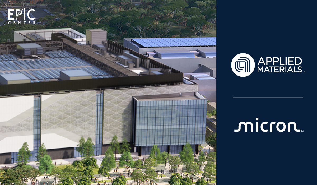
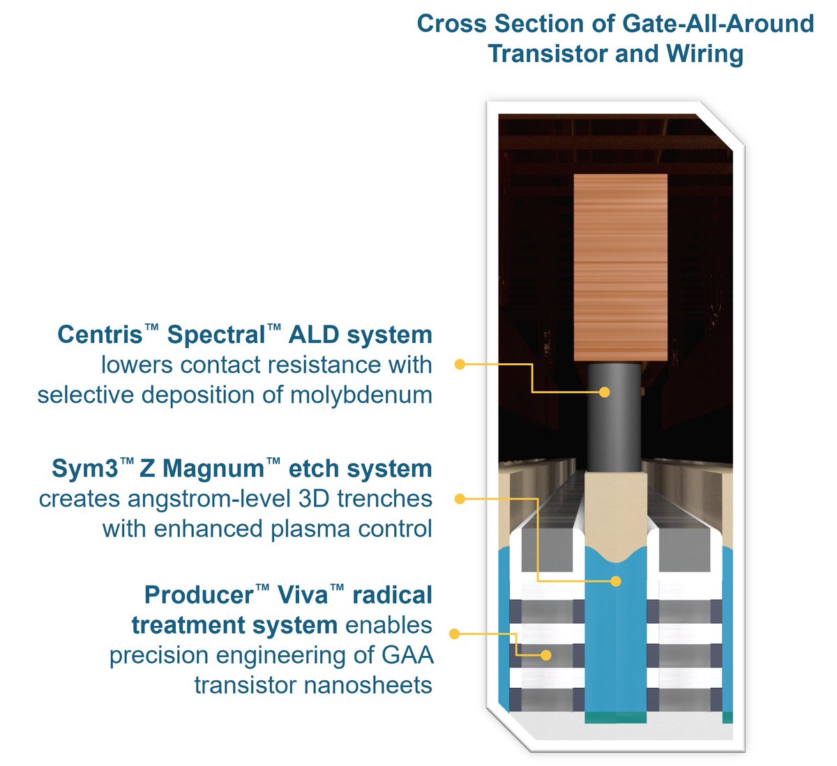
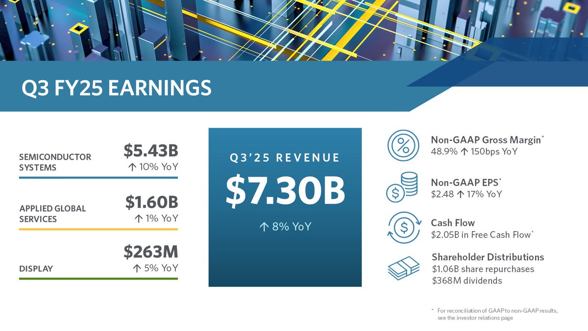
Applied Materials is proud to announce a long-term collaboration agreement with @SKhynix to accelerate the development and deployment of next-generation DRAM and high-bandwidth memory (HBM). Engineers from both companies will work side-by-side at Applied’s EPIC Center in Silicon Valley to advance innovation in materials, process integration and 3D advanced packaging as memory architectures move beyond current production nodes. 
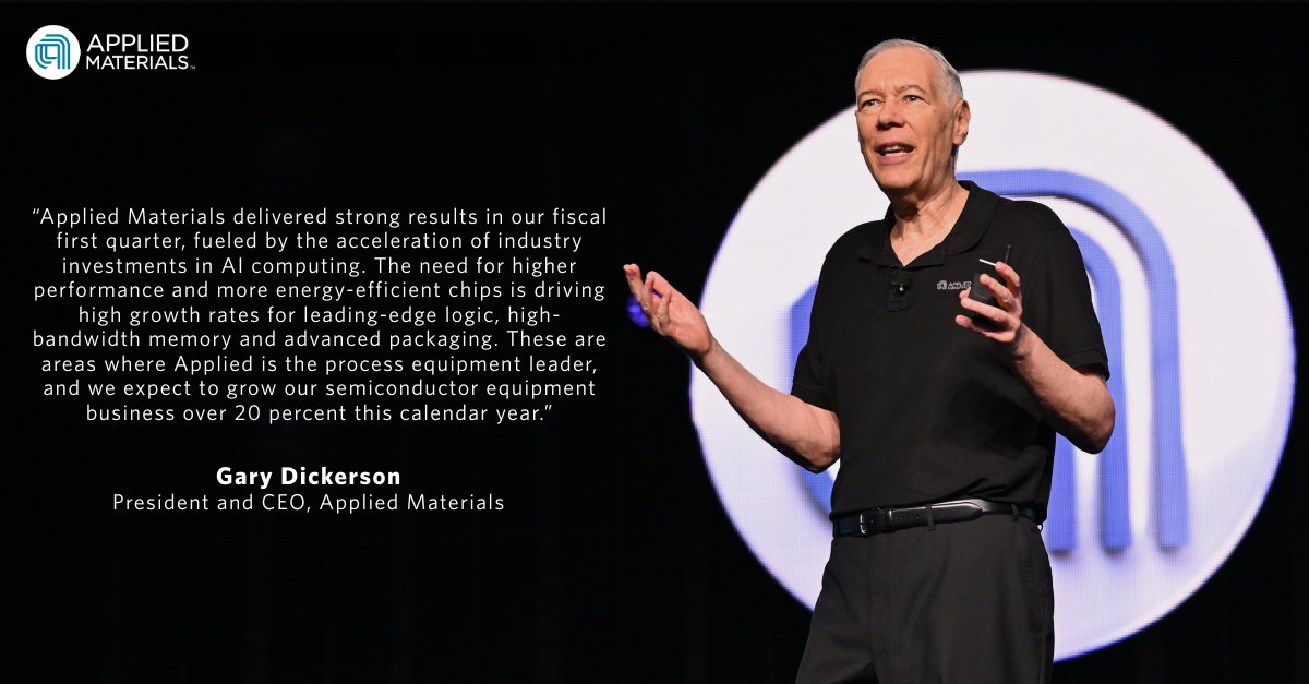
President and CEO Gary Dickerson shared, “Applied Materials and SK hynix share a long history of working together to improve the energy-efficient performance of advanced memory chips through innovations in materials engineering,” He added, “We are excited to have SK hynix join the EPIC Center as a founding partner, and we look forward to driving further breakthroughs together that accelerate commercialization of next-generation DRAM and HBM technologies for the AI era.” Learn more: bit.ly/4rpcuB0
Applied Materials tweet media
English
1
10
77
15.1K
Applied Materials
Applied Materials@Applied4Tech·
We're excited to announce we are working with Micron Technology to develop next-generation DRAM, high-bandwidth memory (HBM) and NAND solutions that increase the energy-efficient performance of AI systems, bringing together advanced R&D capabilities from our EPIC Center in Silicon Valley and Micron’s state-of-the-art innovation center in Boise, Idaho to strengthen the semiconductor innovation pipeline in the United States. Here’s what our CEO, Gary Dickerson, had to say: “Applied Materials and Micron have a long-standing partnership focused on driving higher performance and more energy-efficient advanced memory chips by pushing the boundaries of materials engineering and manufacturing innovation,” said Gary Dickerson, President and CEO of Applied Materials. “We are excited to deepen our collaboration with Micron as a founding partner at the EPIC Center as next-generation memory technologies play an increasingly vital role in the future of AI systems.” Learn more: bit.ly/4byPdrs
Applied Materials tweet media
English
0
8
77
12.1K
Applied Materials
Applied Materials@Applied4Tech·
Pushing AI performance requires increasingly tighter tolerances and extreme precision. Applied's Sym3™ Z Magnum™ conductor etch system extends the proven Sym3 Z platform by bringing plasma and ion control closer to the wafer, delivering angstrom‑level etch control, improving wafer uniformity and enabling faster, more energy‑efficient chips. bit.ly/4kZMKJN
Applied Materials tweet media
English
0
4
21
808
Applied Materials
Applied Materials@Applied4Tech·
Inside every chip, there’s a tiny metal contact, or bridge, that helps electricity move between layers. As chips get smaller and AI demands more speed, these tiny contacts have become a major bottleneck. Applied Materials is enabling the next generation of contact scaling using molybdenum, a material that keeps electricity flowing faster, even at the most advanced nodes. Learn more about our materials engineering expertise: bit.ly/4rsMs0y
Applied Materials tweet media
English
2
3
14
622
Applied Materials
Applied Materials@Applied4Tech·
We reported our Q1 FY26 financial results. A key highlight, accelerated AI adoption and market growth signaling expectations the growth of our semiconductor equipment business by 20% this calendar year. Learn more: bit.ly/4aw9agS
Applied Materials tweet media
English
0
3
17
669
Applied Materials
Applied Materials@Applied4Tech·
Today we reported results for the first quarter of fiscal 2026. Check out this snapshot to learn more about our financial results and business highlights. bit.ly/4aw9agS
Applied Materials tweet media
English
3
4
13
877
Applied Materials
Applied Materials@Applied4Tech·
We are excited to announce that Samsung Electronics will join the new $5 billion Applied Materials EPIC Center in Silicon Valley. Our EPIC Center will open this year as the world’s largest and most advanced facility for collaborative semiconductor process technology and manufacturing equipment R&D. The EPIC center is designed from the ground up to dramatically reduce the time it takes to commercialize breakthrough technologies from early-stage research to full-scale manufacturing. For chipmakers, the EPIC Center will provide earlier access to our R&D portfolio, faster cycles of learning and accelerated transfer of next-generation technologies into high-volume manufacturing. Read the full release here: bit.ly/4tBAOlE
Applied Materials tweet media
English
0
4
31
2K
Applied Materials
Applied Materials@Applied4Tech·
Today we introduced new semiconductor manufacturing systems that boost the performance of leading-edge logic chips at 2nm and beyond. The technologies supercharge AI compute through atomic-scale improvements to the most fundamental electronic building block – the transistor. The new lineup of products include: • Applied Producer™ Viva™ radical treatment system boosts transistor performance with atomic-level precision engineering of the nanosheet surface • Applied Centris™ Sym3™ Z Magnum™ conductor etch system delivers angstrom-level 3D trench profile control to increase silicon nanosheet uniformity and performance • Applied Centris™ Spectral™ Molybdenum ALD system replaces today's tungsten transistor contacts with molybdenum, a new contact metal that lowers electrical resistance at the critical link between transistors and the copper wiring network The technologies supercharge AI compute through atomic-scale improvements to the most fundamental electronic building block – the transistor and are being used now by multiple leading foundry-logic manufacturers. bit.ly/4tsfxdJ
Applied Materials tweet media
English
0
3
26
1.1K
Applied Materials
Applied Materials@Applied4Tech·
Today we reported results for the fourth quarter and full year fiscal 2025. Check out this snapshot to learn more about our financial results and business highlights. bit.ly/3JIXlL7
Applied Materials tweet media
English
1
2
18
1.2K
Applied Materials
Applied Materials@Applied4Tech·
Today, together with Arizona State University, we marked the official opening of the Materials-to-Fab Center, a shared world-class $270 million research, development and prototyping facility inside the university’s MacroTechnology Works at ASU’s Research Park in Tempe. Dr. Prabu Raja, President of the Semiconductor Products Group at Applied Materials, said, “Universities are the foundation of America’s semiconductor innovation pipeline, and we look forward to bringing together ASU’s world-class engineering teams with Applied Materials technologists and ecosystem partners at the Materials-to-Fab Center. These collaborations will focus on accelerating development of new chip technologies that are crucial to U.S. leadership in AI, high-performance computing and other megatrends shaping the future.” Read more: bit.ly/3IOmlAb
Applied Materials tweet media
English
2
5
27
2.8K
Applied Materials
Applied Materials@Applied4Tech·
Today at #SEMICONWest we introduced new semiconductor manufacturing systems that boost the performance of advanced logic and memory chips foundational to AI computing. The new products target three critical areas in the race to deliver ever more powerful AI chips: leading-edge logic including Gate-All-Around (GAA) transistors, high-performance DRAM including high-bandwidth memory (HBM), and advanced packaging to create highly integrated systems-in-a-package that optimize chip performance, power consumption and cost. #MakeItMaterial Read more: bit.ly/4q36OgK
Applied Materials tweet media
English
2
5
22
2.1K
Applied Materials
Applied Materials@Applied4Tech·
We've announced a strategic collaboration with @GlobalFoundries (GF) to establish a state-of-the-art waveguide fabrication facility at GF Singapore to accelerate the emerging photonics inflection driven by AI. The collaboration marks a significant milestone in the evolution of photonics as a foundational technology for next-generation AI applications, including augmented reality (AR) and human-centric digital experiences that require ultra-efficient, lightweight and high-performance optical systems. bit.ly/4mtzEnd
English
0
4
12
1.1K
Applied Materials
Applied Materials@Applied4Tech·
Heading to Arizona for #SEMICONWest? Our team is excited to talk about everything from sustainability to AI to semiconductor industry talent—our focus is to deliver material innovation that changes the world. We look forward to seeing you there! #MakeItMaterial bit.ly/4msXcsk
English
0
2
15
1.1K
Applied Materials
Applied Materials@Applied4Tech·
ICYMI: We recently announced that we're putting more than $200 million into an all-new, state-of-the-art manufacturing facility in Arizona. This facility is going to manufacture the critical components that keep semiconductor equipment running. 🚀 It’s inspiring to be part of the current wave of innovation in chipmaking in the U.S. The future of semiconductor technology? It’s all about materials science innovation. #MakeItMaterial bit.ly/4mIJli8
Applied Materials tweet media
English
3
2
29
1.6K
Applied Materials
Applied Materials@Applied4Tech·
Today we reported results for the third quarter of fiscal 2025. Check out this snapshot to learn more about our financial results and business highlights. bit.ly/3UZE4H4
Applied Materials tweet media
English
0
2
20
1.4K
Applied Materials
Applied Materials@Applied4Tech·
🌟 At Applied Materials, we’ve been building the future for decades—innovating and preparing for something bigger. It’s now our #MaterialMoment. We are excited to be at the heart of innovation bringing you the next wave of technology that will change the world. 🌍 #MakeItMaterial bit.ly/3IefDTn
Applied Materials tweet media
English
0
1
24
1.4K
Applied Materials
Applied Materials@Applied4Tech·
We’re proudly supporting Apple's partnership with Texas Instruments (TI) by supplying American-made chipmaking equipment to TI’s U.S. factories. #MakeItMaterial bit.ly/45jx5xt
Applied Materials tweet media
English
1
8
78
5.5K
Applied Materials
Applied Materials@Applied4Tech·
🌍 At Applied Materials, we’ve been on an incredible journey of innovation and discovery that has led to this moment, our #MaterialMoment. Our innovation in materials science is more than a goal, it’s our passion. It’s our commitment to our employees because the work we do together advances the world’s technology. Are you ready to join us? 🌟 #MakeItMaterial bit.ly/3IefDTn
English
0
1
14
851