
Yay! We made the SEMI-final! ;-)
SEMI@SEMIconex
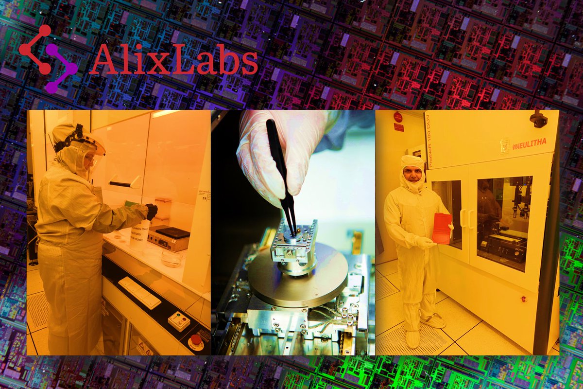
The SEMI #Startups for #Semiconductor #Sustainability program has announced 2023 semifinalists, organizations that will focus on three areas: #circularity, #emissions and #energy efficiency. Learn more about our work to spur more green tech innovation 👉 bit.ly/40vH91Y
English