Masterclass on IC Lithography
You can spend one hour and catch up on the entire arc of semi lithography.
We cover:
- Economics of modern lithography
- what is takes to build a leading-edge fab
- how we evolved from DUV to EUV
- fun stories from history along the way
- where we are going with xLight and Substrate
Check it out!
Chapters:
(00:00) The 13F panic, and today's topic
(02:23) Why the real story is economics, not physics
(06:18) Austin in the clean room: graphene and bunny suits
(10:06) Rock's Law and the $20 billion fab
(18:08) DUV, the Sharpie, and a history of light
(24:58) Multi-patterning, explained with a football field
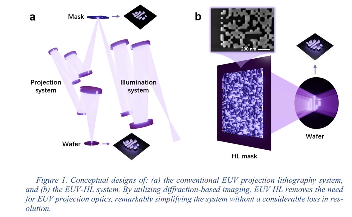
(34:45) How EUV makes 13.5nm light from tin droplets
(41:14) High NA, anamorphic optics, and the half-field tax
(46:45) The startups rethinking lithography: xLight and Substrate
@austinsemis@vikramskryoutube.com/watch?v=WWbEfD…
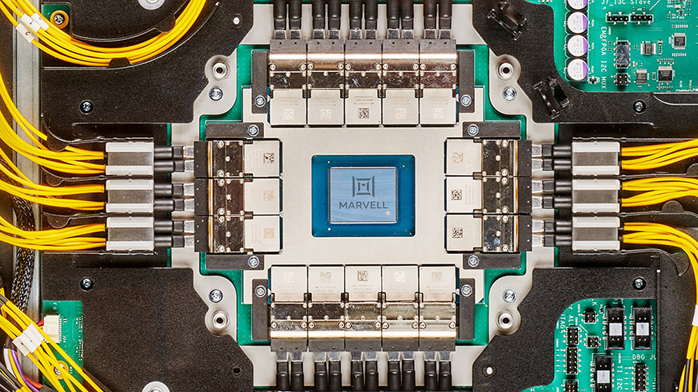
As optics migrate from front-panel modules to near-packaged and co-packaged configurations directly alongside compute die, the manufacturing challenge shifts as well. Testing methods designed for low-volume, custom configurations cannot scale to meet the demands of AI infrastructure production.
In a new article, Senior Director of Product and Test Engineering Andrew Yick makes the case for treating optical test as a first-class manufacturing discipline, applying the same shift-left, design-for-test, and ATE-enabled approaches that have governed high-volume semiconductor production for decades.
The core principle: if it cannot be tested like an integrated circuit, it will not scale like one.
Learn more: mrvl.co/4nzfWsk
HBM’s dominance is not accidental. Technically, it achieves extreme performance through three core elements:
♦️ 3D stacking – multiple DRAM dies vertically stacked to shorten internal data paths
♦️ TSVs (Through-Silicon Vias) – vertical electrical interconnects drilled through silicon
♦️ Ultra-close integration with logic dies (via advanced packaging such as interposers)