Y

13.1K posts

Y banner
Y

Y

@Six28f

普通のサラリーマン

Bergabung Mart 2022
101 Mengikuti1.9K Pengikut
Y me-retweet
五重 黄昏𝕏
五重 黄昏𝕏@arafifniharuwo·
東京大学が作製したAlNショットキーバリアダイオード素子は、AlN系デバイスの中で世界最小のオン抵抗0.34 mΩcm2を示し、逆方向耐圧400 V(最大破壊電界8 MV/cm)を示した。 これはSiの理論限界を大きく凌駕し、SiC、GaNの理論限界に肉薄するもので、インパクトが大きい結果。 t.u-tokyo.ac.jp/press/pr2026-0…
日本語
0
3
22
819
Y
Y@Six28f·
「第32回 半導体・オブ・ザ・イヤー2026」でPFASフリーネガ型ArF液浸レジストが優秀賞を受賞 | 富士フイルム [日本] fujifilm.com/jp/ja/news/lis…
日本語
0
0
2
69
Y
Y@Six28f·
去年の記事ですが、メモメモ。 世界初成功!ハロゲンフリーのプラズマプロセスで 次世代半導体材料を原子レベルで微細に加工・制御 - 名古屋大学研究成果情報 share.google/IH2Dsfefud7YEe…
日本語
0
5
13
2.9K
Y
Y@Six28f·
古河電工、データセンター関連の営業益8.5倍の2000億円へ…「現実的な到達レベルという認識でいる」 | #ニュースイッチ @newswitch_ newswitch.jp/p/49239
日本語
0
0
0
129
ラテン語さん
ラテン語さん@latina_sama·
私は、教養ある人というのは「自分の知識を活かして周りにやさしくする人」だと思っています。
日本語
46
2.7K
22.8K
563.2K
Y
Y@Six28f·
5月も終わりか。速いな。
日本語
0
0
0
36
Y
Y@Six28f·
@nikkeibusiness 経営者の限界でしょう。当たり前です。
日本語
0
0
0
565
日経ビジネス
日経ビジネス@nikkeibusiness·
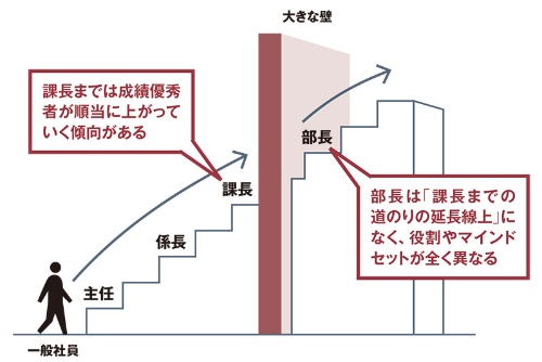
「部長の限界」が「会社の限界」に business.nikkei.com/atcl/seminar/1… 多くの部長は成果を上げるのに必死で、現場のことばかり見ている。経営者が「現場は下に任せて、君は部長の仕事を」と指示するだけでは、状況は改善しない。(2021年7月)
日経ビジネス tweet media
日本語
21
144
1.2K
383.5K
Y me-retweet
Semi Doped
Semi Doped@semidoped·
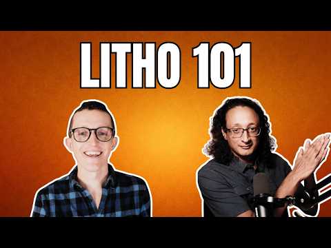
Masterclass on IC Lithography You can spend one hour and catch up on the entire arc of semi lithography. We cover: - Economics of modern lithography - what is takes to build a leading-edge fab - how we evolved from DUV to EUV - fun stories from history along the way - where we are going with xLight and Substrate Check it out! Chapters: (00:00) The 13F panic, and today's topic (02:23) Why the real story is economics, not physics (06:18) Austin in the clean room: graphene and bunny suits (10:06) Rock's Law and the $20 billion fab (18:08) DUV, the Sharpie, and a history of light (24:58) Multi-patterning, explained with a football field (34:45) How EUV makes 13.5nm light from tin droplets (41:14) High NA, anamorphic optics, and the half-field tax (46:45) The startups rethinking lithography: xLight and Substrate @austinsemis @vikramskr youtube.com/watch?v=WWbEfD…
YouTube video
YouTube
English
0
12
64
7.2K
Y
Y@Six28f·
@nekogal21 SOSやったんですね。腰痛なりますもんね。
日本語
0
0
0
66
窓際三等兵
窓際三等兵@nekogal21·
若手社員の頃、おじさんがずっとコーヒー飲んでるのが不思議だったけど謎が解けた。中年はカフェインを摂り続けないと脳が働かないので、ドーピングで鞭打って無理やり動かしてるだけだった。頻繁に席を立ってトイレに向かうおじさん達はサボってる訳でなく、助けて欲しいというサインを発している。
日本語
25
300
2K
151.5K
Y
Y@Six28f·
@saketaro88 ムラムラしますね
日本語
0
0
1
44
飲みりーまん
飲みりーまん@saketaro88·
育休取ることは別に構わんのやが、中途入社してきて頑張らないかんフェーズやのに平気で育休取るのはどうなん? 転職前にわかってたのでは? とムラムラしてます。
日本語
4
1
21
9.5K
Y
Y@Six28f·
@skill___up @litulon 気持ちめっちゃわかります。どうすりゃいいんや。
日本語
0
0
3
53
Y me-retweet
Aaron
Aaron@Aaronwei3n·
Sheesh. $NVDA VR200 Bom Analysis from MS.
Aaron tweet media
English
41
137
919
959.3K
Y me-retweet
Marvell Technology
Marvell Technology@MarvellTech·
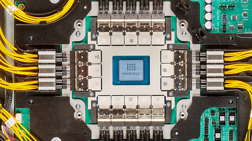
As optics migrate from front-panel modules to near-packaged and co-packaged configurations directly alongside compute die, the manufacturing challenge shifts as well. Testing methods designed for low-volume, custom configurations cannot scale to meet the demands of AI infrastructure production. In a new article, Senior Director of Product and Test Engineering Andrew Yick makes the case for treating optical test as a first-class manufacturing discipline, applying the same shift-left, design-for-test, and ATE-enabled approaches that have governed high-volume semiconductor production for decades. The core principle: if it cannot be tested like an integrated circuit, it will not scale like one. Learn more: mrvl.co/4nzfWsk
Marvell Technology tweet media
English
2
54
449
68.2K
Y me-retweet
SemiVision👁️👁️
SemiVision👁️👁️@semivision_tw·
HBM’s dominance is not accidental. Technically, it achieves extreme performance through three core elements: ♦️ 3D stacking – multiple DRAM dies vertically stacked to shorten internal data paths ♦️ TSVs (Through-Silicon Vias) – vertical electrical interconnects drilled through silicon ♦️ Ultra-close integration with logic dies (via advanced packaging such as interposers)
SemiVision👁️👁️ tweet media
English
1
8
55
3.7K