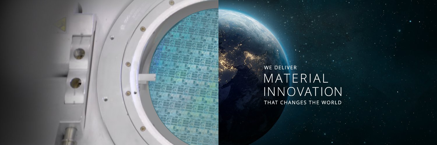
Applied Materials

2.9K posts

Applied Materials banner
Applied Materials

Applied Materials

@Applied4Tech

We deliver material innovation that changes the world.

Santa Clara, California Katılım Ağustos 2009
1.5K Takip Edilen16K Takipçiler
Applied Materials
Applied Materials@Applied4Tech·
Applied Materials has announced that @ASU, @rpi and @StanfordEng will join the company’s EPIC Center in Silicon Valley as inaugural research partners. Through close collaboration with Applied’s scientists and engineers, university teams will engage in high velocity research programs across advanced materials, novel process and device technologies, and chip architecture inflections – leveraging the synergy of academia and industry to accelerate energy efficient innovations for next generation AI chips. ir.appliedmaterials.com/news-releases/…
Applied Materials tweet media
English
2
3
11
843
Applied Materials
Applied Materials@Applied4Tech·
Today Applied Materials announced a new innovation partnership with TSMC to accelerate the development and commercialization of semiconductor technologies required for the next era of AI. Working together at Applied’s EPIC Center in Silicon Valley, the companies will co-innovate to advance materials engineering, equipment innovation, and process integration technologies designed to deliver energy-efficient performance from the data center to the edge. “Applied and TSMC share a long history of deep collaboration built on trust and a shared commitment to advancing innovation at the leading edge of semiconductor technology,” said Gary Dickerson, President and CEO of Applied Materials. “By bringing our teams together at the EPIC Center, we are strengthening that partnership and accelerating the development of technologies to address the unprecedented complexity driving the chipmaking roadmap.” Learn more: bit.ly/3Ryr9xj
Applied Materials tweet media
English
2
7
29
1.9K
Applied Materials
Applied Materials@Applied4Tech·
Today we announced we have entered into a definitive agreement with ASMPT SEMI Solutions to acquire its ASMPT NEXX, Inc. business, a leading supplier of large-area advanced packaging deposition equipment for the semiconductor industry. The addition of the NEXX team and products will broaden Applied’s portfolio of panel-level advanced packaging technologies which are designed to enable chipmakers and systems companies to build larger-body AI accelerators for higher energy-efficient performance. Learn more: bit.ly/3P7fcxM
Applied Materials tweet media
English
7
15
105
20.4K
Applied Materials
Applied Materials@Applied4Tech·
As AI drives demand for faster, more energy‑efficient chips, transistor customization is becoming just as important as scaling. The Applied Materials Trillium™ system enables chipmakers to precisely engineer materials at the atomic level, allowing transistor performance to be tuned for specific AI workloads. By combining advanced deposition, integration and process control in a single platform, Trillium helps speed development of next‑generation devices while delivering better power, performance and yield at leading‑edge nodes - a key step toward more flexible, application‑optimized semiconductors in the AI era. Learn more: bit.ly/4tu72id #MakeItMaterial
Applied Materials tweet media
English
6
7
42
2.3K
Applied Materials
Applied Materials@Applied4Tech·
Want to learn more about Applied's material innovation in transistors but missed our recent Leading the Future of Logic Master Class? Watch this video where we describe how shallow trench isolation enables increased transistor speed and power efficiency. #MakeItMaterial
English
4
2
10
919
Applied Materials
Applied Materials@Applied4Tech·
Today we announced that Advantest Corporation, a leading semiconductor test equipment supplier, will join Applied’s EPIC platform as an innovation partner to strengthen the links between front-end manufacturing technologies and back-end testing of chips and packages, helping chipmakers bring new designs to market faster. To support this partnership, Advantest has established a new, state-of-the-art Innovation Center on Applied Materials’ R&D campus in Silicon Valley, that will seamlessly connect with Applied’s EPIC Center. “Applied Materials designed the EPIC platform to dramatically accelerate the commercialization of next-generation semiconductors by co-locating and co-innovating with our customers and partners,” said Gary Dickerson, President and CEO of Applied Materials. “By collaborating side-by-side with Advantest, we can develop solutions that enable chipmakers to optimize end-to-end semiconductor production flows and bring new designs to market faster and more efficiently.” Learn more about the partnership: ir.appliedmaterials.com/news-releases/…
Applied Materials tweet media
English
1
2
16
690
Applied Materials
Applied Materials@Applied4Tech·
AI is driving the semiconductor industry into the angstrom era. Next‑generation AI GPUs in development are expected to integrate 300+ billion transistors on a single chip, pushing performance, power efficiency, and manufacturability to new limits. Applied Materials’ Producer™ Precision™ Selective Nitride PECVD system addresses one of the toughest challenges in advanced GAA logic: preserving shallow trench isolation (STI) at atomic‑scale dimensions. Using an industry‑first selective bottom‑up deposition, the system places dense silicon nitride only where needed, protecting isolation through 500+ downstream process steps. The result: lower parasitic capacitance, reduced leakage, and improved performance‑per‑watt without damaging sensitive underlayers - all thanks to low‑temperature processing. Now being adopted by leading foundry‑logic manufacturers at 2nm and beyond, Precision Selective Nitride highlights how materials engineering, not lithography alone, is driving the next phase of chip scaling. Learn more: bit.ly/4cf85Lx #Semiconductors #AIHardware #AdvancedLogic #GAA #2nm #ChipManufacturing #AppliedMaterials #ProcessTechnology
Applied Materials tweet media
English
1
2
15
761
Applied Materials
Applied Materials@Applied4Tech·
We’re excited to introduce two new deposition systems designed to meet the extreme complexity of Gate-All-Around (GAA) architectures: 🔹Precision™ Selective Nitride PECVD 🔹Trillium™ ALD Together, these systems give leading logic manufacturers the materials precision needed to deliver faster, more power‑efficient chips at the most advanced nodes. Learn more: bit.ly/4cf85Lx
Applied Materials tweet media
English
2
8
41
4.3K
Applied Materials
Applied Materials@Applied4Tech·
Welcome back to Applied’s semiconductor chip city where we talk about each piece of the city works together to make a real, meaningful difference. Imagine multilayer metal highways connecting every part of a chip. That’s our focus for today: interconnects. 🛣️ Interconnects route signals across and between layers of metal at lightning speed. These interconnects are like a highway of innovation within our semiconductor chip city. Learn more about our Interconnect solutions: bit.ly/3NWEAG5 We deliver material innovation that changes the world. #MakeItMaterial
English
1
1
7
633
Applied Materials
Applied Materials@Applied4Tech·
Applied Materials is proud to announce a long-term collaboration agreement with @SKhynix to accelerate the development and deployment of next-generation DRAM and high-bandwidth memory (HBM). Engineers from both companies will work side-by-side at Applied’s EPIC Center in Silicon Valley to advance innovation in materials, process integration and 3D advanced packaging as memory architectures move beyond current production nodes. President and CEO Gary Dickerson shared, “Applied Materials and SK hynix share a long history of working together to improve the energy-efficient performance of advanced memory chips through innovations in materials engineering,” He added, “We are excited to have SK hynix join the EPIC Center as a founding partner, and we look forward to driving further breakthroughs together that accelerate commercialization of next-generation DRAM and HBM technologies for the AI era.” Learn more: bit.ly/4rpcuB0
Applied Materials tweet media
English
1
11
81
15.5K
Applied Materials
Applied Materials@Applied4Tech·
We're excited to announce we are working with Micron Technology to develop next-generation DRAM, high-bandwidth memory (HBM) and NAND solutions that increase the energy-efficient performance of AI systems, bringing together advanced R&D capabilities from our EPIC Center in Silicon Valley and Micron’s state-of-the-art innovation center in Boise, Idaho to strengthen the semiconductor innovation pipeline in the United States. Here’s what our CEO, Gary Dickerson, had to say: “Applied Materials and Micron have a long-standing partnership focused on driving higher performance and more energy-efficient advanced memory chips by pushing the boundaries of materials engineering and manufacturing innovation,” said Gary Dickerson, President and CEO of Applied Materials. “We are excited to deepen our collaboration with Micron as a founding partner at the EPIC Center as next-generation memory technologies play an increasingly vital role in the future of AI systems.” Learn more: bit.ly/4byPdrs
Applied Materials tweet media
English
0
9
78
12.8K
Applied Materials
Applied Materials@Applied4Tech·
Pushing AI performance requires increasingly tighter tolerances and extreme precision. Applied's Sym3™ Z Magnum™ conductor etch system extends the proven Sym3 Z platform by bringing plasma and ion control closer to the wafer, delivering angstrom‑level etch control, improving wafer uniformity and enabling faster, more energy‑efficient chips. bit.ly/4kZMKJN
Applied Materials tweet media
English
0
5
23
984
Applied Materials
Applied Materials@Applied4Tech·
Inside every chip, there’s a tiny metal contact, or bridge, that helps electricity move between layers. As chips get smaller and AI demands more speed, these tiny contacts have become a major bottleneck. Applied Materials is enabling the next generation of contact scaling using molybdenum, a material that keeps electricity flowing faster, even at the most advanced nodes. Learn more about our materials engineering expertise: bit.ly/4rsMs0y
Applied Materials tweet media
English
3
4
15
768
Applied Materials
Applied Materials@Applied4Tech·
We reported our Q1 FY26 financial results. A key highlight, accelerated AI adoption and market growth signaling expectations the growth of our semiconductor equipment business by 20% this calendar year. Learn more: bit.ly/4aw9agS
Applied Materials tweet media
English
0
3
18
782
Applied Materials
Applied Materials@Applied4Tech·
Today we reported results for the first quarter of fiscal 2026. Check out this snapshot to learn more about our financial results and business highlights. bit.ly/4aw9agS
Applied Materials tweet media
English
3
4
13
975
Applied Materials
Applied Materials@Applied4Tech·
We are excited to announce that Samsung Electronics will join the new $5 billion Applied Materials EPIC Center in Silicon Valley. Our EPIC Center will open this year as the world’s largest and most advanced facility for collaborative semiconductor process technology and manufacturing equipment R&D. The EPIC center is designed from the ground up to dramatically reduce the time it takes to commercialize breakthrough technologies from early-stage research to full-scale manufacturing. For chipmakers, the EPIC Center will provide earlier access to our R&D portfolio, faster cycles of learning and accelerated transfer of next-generation technologies into high-volume manufacturing. Read the full release here: bit.ly/4tBAOlE
Applied Materials tweet media
English
0
4
31
2.1K
Applied Materials
Applied Materials@Applied4Tech·
Today we introduced new semiconductor manufacturing systems that boost the performance of leading-edge logic chips at 2nm and beyond. The technologies supercharge AI compute through atomic-scale improvements to the most fundamental electronic building block – the transistor. The new lineup of products include: • Applied Producer™ Viva™ radical treatment system boosts transistor performance with atomic-level precision engineering of the nanosheet surface • Applied Centris™ Sym3™ Z Magnum™ conductor etch system delivers angstrom-level 3D trench profile control to increase silicon nanosheet uniformity and performance • Applied Centris™ Spectral™ Molybdenum ALD system replaces today's tungsten transistor contacts with molybdenum, a new contact metal that lowers electrical resistance at the critical link between transistors and the copper wiring network The technologies supercharge AI compute through atomic-scale improvements to the most fundamental electronic building block – the transistor and are being used now by multiple leading foundry-logic manufacturers. bit.ly/4tsfxdJ
Applied Materials tweet media
English
0
3
26
1.2K
Applied Materials
Applied Materials@Applied4Tech·
Today we reported results for the fourth quarter and full year fiscal 2025. Check out this snapshot to learn more about our financial results and business highlights. bit.ly/3JIXlL7
Applied Materials tweet media
English
1
2
18
1.3K