ChipIN Centre retweetledi

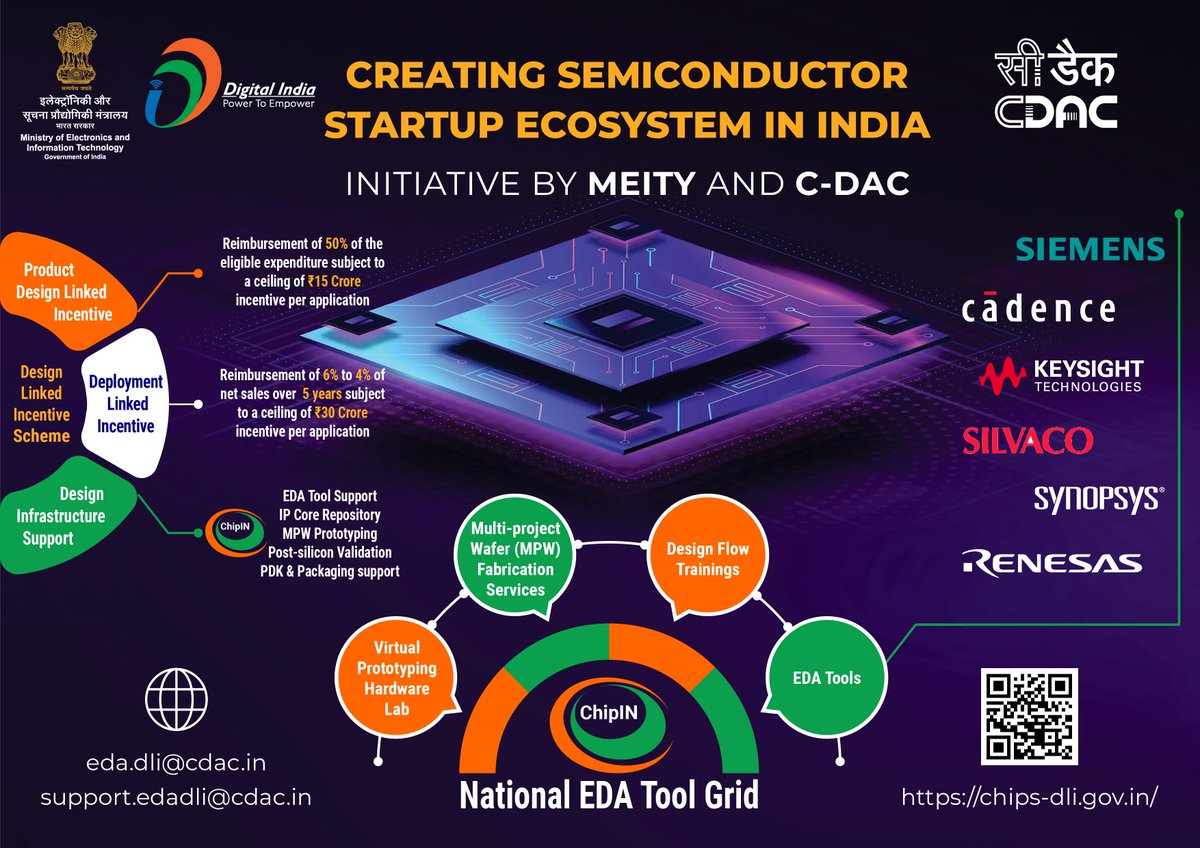
💠Government of India creating enabling environment for Semiconductor Design Community with direct access to National Chip Design Infrastructure
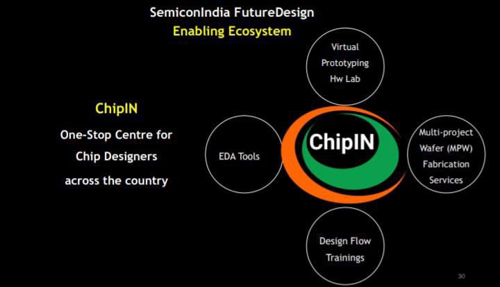
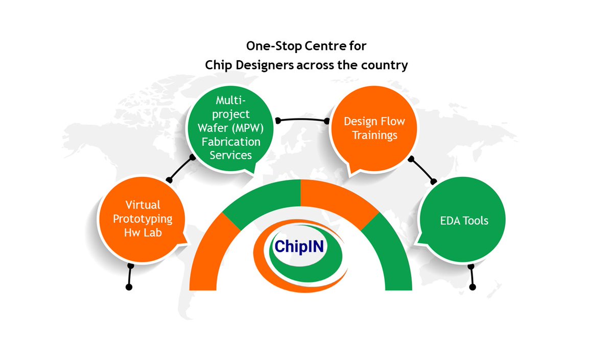
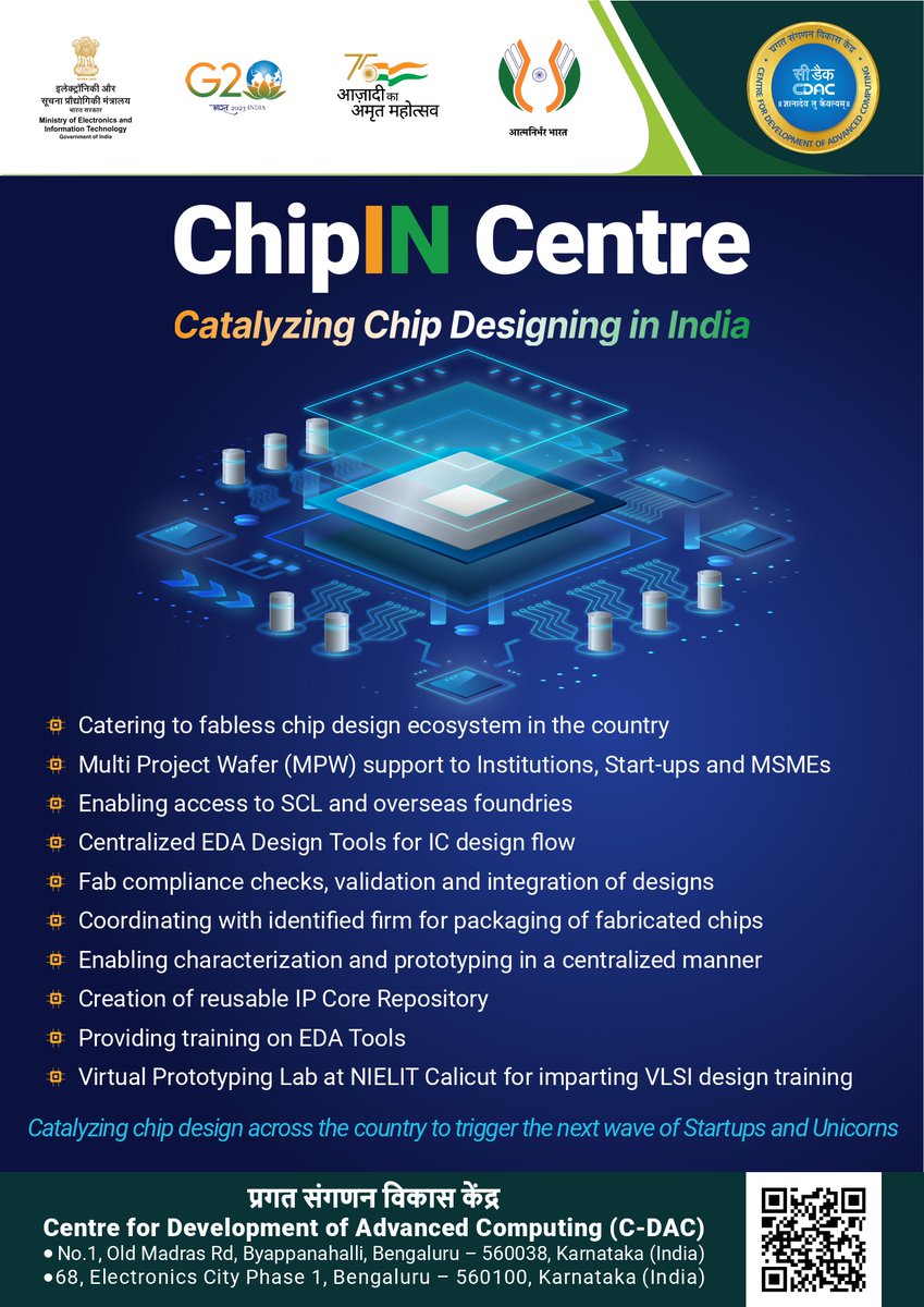
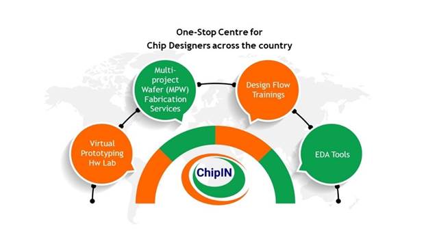
💠ChipIN (CDAC), one-stop centre for chip designers nationwide, gets momentum with extended support from semiconductor industry leader Siemens EDA
💠20,000+ students from over 250 academic institutions gaining access of EDA tools from Siemens under C2S Programme; ChipIN centre to benefit 85,000 B. Tech, M. Tech, & PhD Students in 5 years
💠Companies approved under the DLI Scheme & C2S Programme to also gain access to Veloce hardware verification solution from Siemens at C-DAC Trivandrum
💠Compute facility to feature 128 CPU cores and a capacity of 640 million gates, helping them address their SoC validation challenges
Read here: pib.gov.in/PressReleasePa…


English