Sabitlenmiş Tweet
Marc
3.7K posts

Marc
@MarcvdField
Sport, muziek, comedy, beurs, politiek & games
Amsterdam, Nederland Katılım Ocak 2011
269 Takip Edilen95 Takipçiler
@JDB_trading Sterke bedrijven zoals $META, $MSFT en $ADYEN traden op historisch aantrekkelijke multiples. Hoe kijk jij met TA ogen naar deze namen? Als je er een of meerdere uit zou willen lichten zou dat leuk zijn! Fijne dag Jan :)
Nederlands

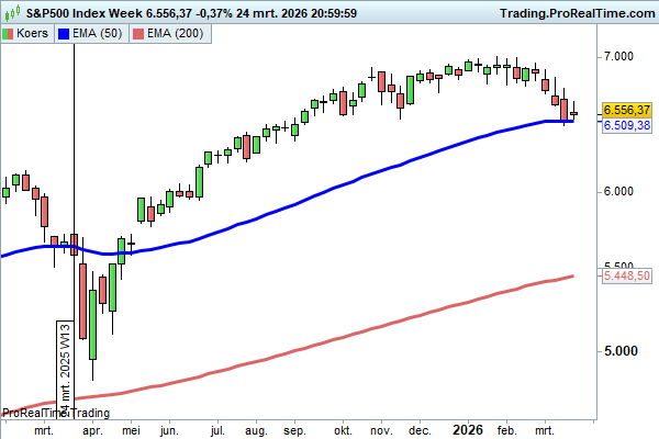
Eindelijk een beetje capitulatie gezien afgelopen vrijdag. Geen garantie voor een bodem, maar naar mijn idee is het nog steeds een bullmarket. Die kraakt pas bij doorbraak lange MA’s (MA20 maand + 2-maands). Het lastige gedeelte is altijd de draai van bull- naar bearmarket, maar daar nu op speculeren lijkt mij te voorbarig.
Anderzijds wil je een doorbraak MA20 week + 50-61.8% retracement zien voor meer bullish momentum! Oftewel, te vroeg voor conclusies, maar ik blijf vooralsnog in het bullishe kamp.
Subu Trade@SubuTrade
$SPY Put Volume spiked on Friday. Previous spikes came close to marking bottoms for the S&P 500. Will this time be different?
Nederlands
@joecarlsonshow Short form content is extremely bad for your brain (+mental health) and super addictive (dopamine). I would say it is the new form of smoking…
English

The reason that Meta is not Big Tobacco is because their product is completely different.
Nicotine is objectively more addictive than social media by multiples. Nicotine is a physical product that enters into the blood stream, crosses the blood-brain barrier, and physically causes a release of dopamine at a speed and level your body cannot naturally produce. It’s literally a physical product that physically changes your biology and creates physical dependency.
Scientists continually rank nicotine as one of the most addicting substances they study.
Social media is not nearly as addictive. The capture rate (the percentage of people that get addicted) is multiples less, the withdrawal profile is far less severe, and social media creates no physical dependency and doesn’t physically harm the body.
Social media companies design their products to be engaging as possible, with features like infinite scroll. But I don’t believe that rises anywhere close to the level of physical dependency and damage that big tobacco does.
It’s also worth pointing out that social media has many great use cases and when done in moderate amounts. With moderation people can network, communicate, learn, be inspired, and be entertained on social media. I don’t believe there are such positive benefits to big tobacco products, even in moderate amounts.
English
@JDB_trading Waar leg je de stoploss volgens jouw regels bij deze? Short gaan bij ema50 blauwe lijn. Koersdoel ema 200 rode lijn. Stoploss X % boven instap? Hoe bepaal jij het? Thx :)
Nederlands
$RHM deze begint een beetje op gang te komen!
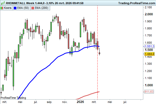
JDB@JDB_trading
$RHM ja, deze ga ik short als die onder EMA50 week sluit straks.
Nederlands
@ZS_Voetbal Is toch duidelijk waarom. Hij zakte zo erg door de mand tijdens het EK. Wedstrijd tegen Oostenrijk als dieptepunt met wissel als ik mij goed herinner? Eredivisie is zijn max, te matig voor oranje.
Nederlands
Nederlands
@JDB_trading Moet het scenario zo 1 op 1 lopen? Kan het niet ook in grote lijnen hetzelfde zijn maar timeframe iets anders?
Nederlands
Marc retweetledi

1. Gasvoorraad op 6.2%.
2. Straat van Hormuz gesloten.
3. Irak, Qatar, Koeweit en Bahrein verklaarden force majeure.
4. Grote productieverlagingen in Saudi-Arabië en de VAE.
5. Één van de grootste raffinaderijen van de VS in brand.
6. VS wenst uitruil LNG met handelsakkoord.
7. Noorwegen produceert op maximale capaciteit.
8. Nederlandse benzine, gas (!) en elektriciteit zijn zo ongeveer de duurste in de wereld.
9. We gooien nog altijd onze gasputten dicht.
Tijd voor Den Haag dit serieus te nemen.
Jitse Groen@jitsegroen
De Nederlandse regering zal gedwongen worden de visionaire leegte waarmee men nu denkt de wereldproblematiek weg te wensen te vervangen door een strategie omtrent het eigen gas en bijbehorende energie onafhankelijkheid. De wal keert het schip wel, al had ik liever gezien dat er iemand in de stuurhut zat en we mijlenver van de kust waren gebleven.
Nederlands

Qatar just declared force majeure on LNG exports due to the Middle East crisis.
Is this "energy security" or just expensive hypocrisy?
#EnergySovereignty #GroningenGas #Energierekening #EnergyCrisis #TTF #Nederland #LNG
English
Marc retweetledi
This is honestly just a terrible development. Part of the unique value of the public markets is liquidity. Making it so companies are required to update their investors less frequent means we are moving towards opaque, confusion, and lack of data.
And there’s nothing “long term” about getting less frequent updates. One of the most long term focused companies ever is Costco, which releases KPIs *monthly*.
Removing the quarterly reporting period will just give investors less data to work with and make it so insiders can sell out of a stock long before the public is aware of the problems.
unusual_whales@unusual_whales
BREAKING: The Securities and Exchange Commission is preparing a proposal to eliminate the quarterly earnings report requirement and instead give companies the option to share results twice a year, per WSJ
English

Marc retweetledi
De EU die wil dat Nederlanders meer gaan beleggen terwijl de Nederlandse overheid dat de facto onmogelijk wil maken legt de incompetentie van het landsbestuur wel aardig bloot denk ik 🇪🇺🇳🇱, om over de kwaliteit van onze media (box3?) nog maar te zwijgen. rtl.nl/nieuws/economi…
Nederlands
Lmaooo, who’s running the socials of this account?! The intern going crazy 😭🫣
The White House@WhiteHouse
OPERATION EPIC FURY • Destroy Iran’s missile arsenal. • Destroy their navy. • Ensure they NEVER get a nuclear weapon. Locked in.
English
@NicoInberg Merk het al langere tijd op. Niet alleen nu mbt chippers. Die lange AI teksten in mijn timeline word ik niet blij van. Als ik dat wil lezen ga ik zelf wel nr gemini. Just some feedback 👍🏼
Nederlands
@MarcvdField Ik ben technisch minder onderlegd dus dan help ik jullie zo :)
Nederlands
Hierdoor trappen ze Besi erin vandaag. Mogelijke vertraging introductie Hybrid Bonding. Voor wat het waard is.
Dikte van volgende generatie HBM mogelijk groter
In de halfgeleiderindustrie wordt gesproken over het versoepelen van de diktestandaard voor toekomstige generaties High Bandwidth Memory (HBM). Voor HBM4 ligt de standaard op 775 micrometer, maar voor toekomstige generaties zoals HBM4E en HBM5 wordt nu een dikte van 825 tot meer dan 900 micrometer besproken.
De belangrijkste reden hiervoor is dat toekomstige HBM-chips 20 DRAM-lagen gestapeld krijgen, waardoor het steeds moeilijker wordt om de chips dun genoeg te houden met bestaande technologie.
Daarnaast speelt de ontwikkeling van nieuwe 3D-chipverpakkingstechnologie van TSMC (SoIC) een rol. Deze technologie maakt systemchips dikker, waardoor het noodzakelijk wordt dat ook HBM-dikte iets toeneemt.
Een mogelijke consequentie is dat de adoptie van hybrid bonding, een geavanceerde maar complexe techniek om chips dunner te maken, kan vertragen. Deze technologie is technisch lastig en duur, en wordt momenteel nog niet op grote schaal gebruikt.
Als de diktestandaard inderdaad wordt versoepeld, kunnen geheugenfabrikanten zoals Samsung, SK Hynix en Micron waarschijnlijk blijven werken met de huidige thermocompression bonding (TC bonding) in plaats van over te stappen op hybrid bonding.
Kort gezegd:
De industrie overweegt dikkere HBM-chips om 20-laagse geheugenstacks mogelijk te maken. Dit zou de noodzaak voor complexere technieken zoals hybrid bonding verminderen.
Jukan@jukan05
Next-Gen HBM Thickness Relaxation Gains Momentum… A Blow to Hybrid Bonding Major semiconductor companies are reportedly in discussions to relax the thickness standard for next-generation high-bandwidth memory (HBM), which requires 20-layer stacking. Figures ranging from 825 to 900 micrometers (μm) and above are being floated — surpassing the 775μm thickness of HBM4 (6th-generation HBM), which is set for full commercialization this year. According to ZDNet Korea's reporting as of the 6th, participants in JEDEC (the Joint Electron Device Engineering Council) are actively discussing a significant relaxation of thickness standards for next-generation HBM. Next-Gen HBM Thickness Standard: Discussions Reach 825–900μm and Beyond HBM is a next-generation memory built by vertically stacking multiple DRAM dies and connecting them via microscopic bumps. Through HBM3E, the thickness standard had been held at 720μm, but it was raised to 775μm with HBM4, largely due to the increased stack count of 12 and 16 layers — up from 8 and 12 in the previous generation. Now, the industry is discussing further relaxation of thickness standards for next-generation HBM — namely HBM4E and HBM5 — which will stack DRAM in 20 layers. The figures currently under discussion range from 825μm to over 900μm. Should the standard be set above 900μm, the increase would substantially exceed any prior jump. "JEDEC needs to finalize key standards one to one-and-a-half years before a product reaches commercialization, so discussions around next-gen HBM thickness are very active right now," said one semiconductor industry official. "Figures above 900μm are already being thrown around." JEDEC is the international standards body for semiconductor products. Its membership includes memory companies such as Samsung Electronics, SK Hynix, and Micron, as well as major global semiconductor firms including Intel, TSMC, NVIDIA, and AMD. Historically, the industry has been extremely strict about limiting HBM thickness increases. If HBM were allowed to grow thicker without constraint, it would become increasingly difficult to match the thickness of system semiconductors — such as GPUs — that are integrated horizontally alongside it. Excessive spacing between DRAM layers also lengthens data transmission paths, degrading performance and efficiency. As a result, memory companies have pursued a range of technologies to keep HBM thin, most notably thinning processes that grind down the backside of core DRAM dies, and bonding technologies that reduce inter-die spacing. Both Memory and Foundry Players Want Thickness Relaxation Despite these efforts, there are two primary reasons why the industry is now actively discussing relaxing the thickness standard for next-generation HBM. The first is the shift to 20-layer stacking. Existing thinning processes and inter-die bonding technologies are approaching their limits in terms of how thin HBM can realistically be made. The packaging roadmap of TSMC, a leading foundry, is also a contributing factor. TSMC currently holds a near-monopoly on 2.5D packaging (CoWoS), which integrates HBM and GPUs into a single AI accelerator. CoWoS uses a wide interposer inserted between the chip and substrate to enhance packaging performance. TSMC's next step beyond 2.5D packaging is SoIC (System-on-Integrated Chips), which vertically stacks system semiconductors at extremely fine pitch in a true 3D configuration. In AI accelerator applications, TSMC-SoIC would combine the stacked system semiconductor with HBM. When TSMC-SoIC is applied, the thickness of the system semiconductor increases by tens of micrometers or more beyond the current 775μm baseline — making a corresponding relaxation of HBM thickness standards essentially inevitable. NVIDIA and Amazon Web Services (AWS) are among the companies reportedly planning to adopt TSMC-SoIC. "The need for next-gen HBM thickness relaxation isn't coming from memory suppliers alone — foundry players have a stake in it too," said one industry official. "It's too early to say definitively whether it will be adopted, but discussions are clearly happening among major players." Industry: "Demand for Hybrid Bonding Could Decline" Industry observers interpret these discussions as a factor that could slow the adoption of next-generation bonding processes such as hybrid bonding. Bonding refers to the process of joining individual DRAM dies within an HBM stack; currently, the dominant method is TC (thermocompression) bonding, which uses heat and pressure. Hybrid bonding directly joins the copper interconnects of chips and wafers, eliminating the bumps between DRAM layers and effectively reducing inter-die spacing to near zero — making it highly advantageous for reducing overall HBM package thickness. However, hybrid bonding is technically extremely challenging. It requires: complete removal of microscopic surface contaminants to achieve seamless chip-to-chip bonding; CMP (chemical mechanical planarization) to achieve a perfectly smooth chip surface; and high alignment precision to ensure accurate mating of each copper pad. Yield can also drop sharply when bonding all 20 dies in sequence. As a result, while major memory companies have continued to research and develop hybrid bonding, none have yet applied it in mass production of HBM. Even Samsung Electronics — the most aggressive developer of hybrid bonding — is only expected to incorporate the technology partially, and at the earliest in HBM4E 16-layer configurations. In this context, if next-gen HBM thickness standards are relaxed, memory companies are likely to continue mass-producing HBM using TC bonders. "There's a view in the industry that even a 50μm relaxation in HBM thickness would be sufficient to enable 20-layer stacking," said one industry official. "And since introducing hybrid bonding would require full replacement of existing equipment at enormous cost, my understanding is that memory companies are broadly in favor of relaxing the next-gen HBM thickness standard."
Nederlands