Nanonics Imaging
146 posts

Nanonics Imaging
@Nanonics
Unique AFM-Raman-TERS, NSOM and MultiProbe SPM with optical integration.
Israel, Jerusalem Katılım Mayıs 2009
493 Takip Edilen263 Takipçiler

Mapping in-situ electrochemistry of batteries has been significantly advanced by applying the important Nanonics AFM-SECM Raman breakthrough. See the work done by Nanonics customers from Wayne State University. pubs.acs.org/doi/abs/10.102…
English
Cantilevered glass AFM sensing probes were pioneered by Nanonics and today Nanonics has 25 years of experience in a variety of functional applications of such probes. Read more about AFM SECM Raman:
nanonics.co.il/literature/sin…
English
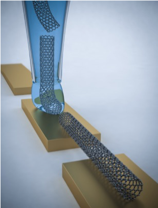
Highly conductive copper pillars for 3D Additive Chemistry have been elegantly implemented with a Nanonics Imaging tuning fork. See details...onlinelibrary.wiley.com/doi/abs/10.100…
English
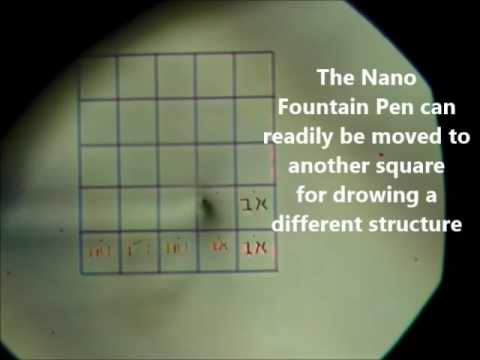
Carcinoma progression is followed using chemical barcode chips produced by Nanonics exclusive Fountain Pen Nanolithography. For more details:
nature.com/articles/s4146…
English
Environmental Control Chambers for Scanned Probe Microscopy youtu.be/5h8CnSpSYHo via @YouTube
YouTube
English
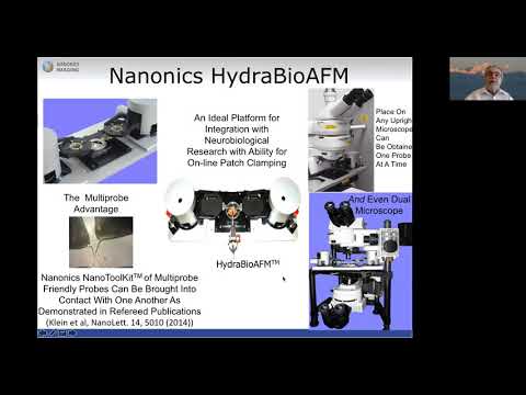
The Hydra BioAFM Nanonics' system. youtu.be/m7daF451OQk via @YouTube
YouTube
Nanonics Continues Effective Support for Customers In Spite of Coronavirus.
English
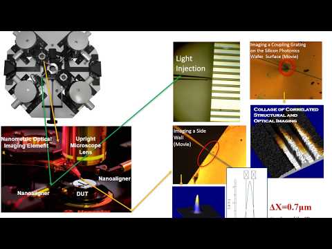
Optical/Structural Nano Characterization of Silicon Photonic Devices and Silicon Chips.
youtu.be/iD2NEMWBlTI via @YouTube
YouTube
English
Nano/Micro Refractive Index Profiling Correlated With Structural Chemical Alterations youtu.be/krLw52L5Fp4 via @YouTube
YouTube
English
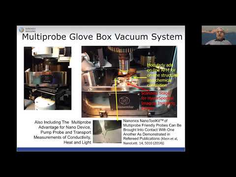
Nanonics Multifunctional Scanning Probe System for vacuum and cryogenic applications.

English
Scanning Probe Microscopy Nanonics system with two probes and two nanoaligners installed in Nanjing University.
English
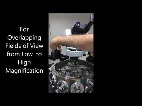
Take a look at the Nanonics' exclusive development of four (4) independently SPM probes in action!!!!
youtube.com/watch?time_con…
nanonics.co.il/solutions/nsom…
YouTube
English
Read this great paper on Photon force microscopy (PiFM) .
nanonics.co.il/news-and-newsl…
English