RayPCB

10.9K posts

RayPCB banner
RayPCB

RayPCB

@RaymingTech

RAYPCB | Since 2005 🌍 🔌 Premium PCB Manufacturing ⚡ Reliable PCB Assembly (PCBA) 💡 Contract EMS Supplier ✨ Fast Turnkey Solutions | Global Shipping

shenzhen Katılım Ocak 2017
4.2K Takip Edilen3K Takipçiler
RayPCB
RayPCB@RaymingTech·
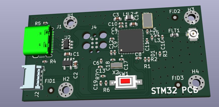
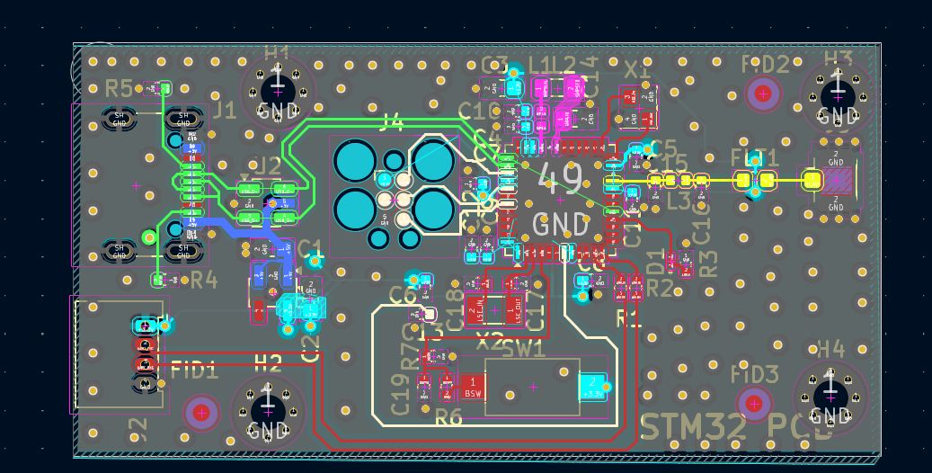
From theory to practice: my first custom STM32WB55 board with Bluetooth connectivity. 🛠️ After following Phil’s Lab STM32 Bluetooth Hardware Design series, I reinforced each step by designing and laying out my own board. Here’s what went into it: Design highlights: • Complete schematic design • STM32WB55 (2.4 GHz Bluetooth MCU) • LDO regulator (5V → 3.3V, MIC5365) • RF low-pass filter + u.FL antenna connector • USB-C interface with CC resistors • 32.768 kHz (LSE) & 32 MHz (HSE) crystals • SWD interface for debugging/programming • Proper power decoupling PCB layout (2-layer board): • Component placement • Power and signal routing • First attempt at RF constraints Key learnings: • RF routing rules (controlled impedance, ground plane continuity) • Power management (LDO, decoupling, stability) • Designing around a Bluetooth-enabled STM32 MCU • Passive component selection (capacitors, resistors – sizing & roles) • Reading and applying datasheet information • PCB layout best practices ⚠️ This is my first design – plenty of room for improvement, especially on the RF and layout side. But that’s exactly how we grow. Would love to hear your tips or resources for improving RF design on 2-layer boards! 👇
RayPCB tweet mediaRayPCB tweet mediaRayPCB tweet media
English
1
0
1
95
RayPCB
RayPCB@RaymingTech·
15.6-inch LCD screen fixture lamination process RAYPCB
English
0
0
4
512
RayPCB
RayPCB@RaymingTech·
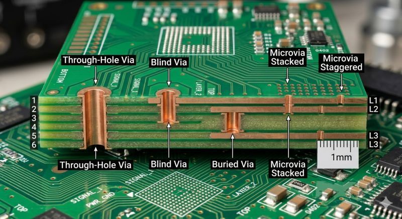
PCB Via Structures: Through Hole vs Blind/Buried vs Stacked vs Staggered Microvias
RayPCB tweet media
English
6
34
350
29.6K
RayPCB
RayPCB@RaymingTech·
This is exactly why a thermal camera can be such a valuable debugging tool. The reference schematic, along with the datasheet, offers some clues about why that resistor is included — it appears the chip has a very simple built-in regulator of some kind. You can check out the datasheet here: laskakit.cz/user/related_f… If you want, I can also make it: more technical, more polished/professional, or more punchy and engaging for LinkedIn.
RayPCB tweet media
English
6
13
98
6.5K
RayPCB
RayPCB@RaymingTech·
3D print PCB circuit board box
Română
0
0
11
3.7K
RayPCB
RayPCB@RaymingTech·
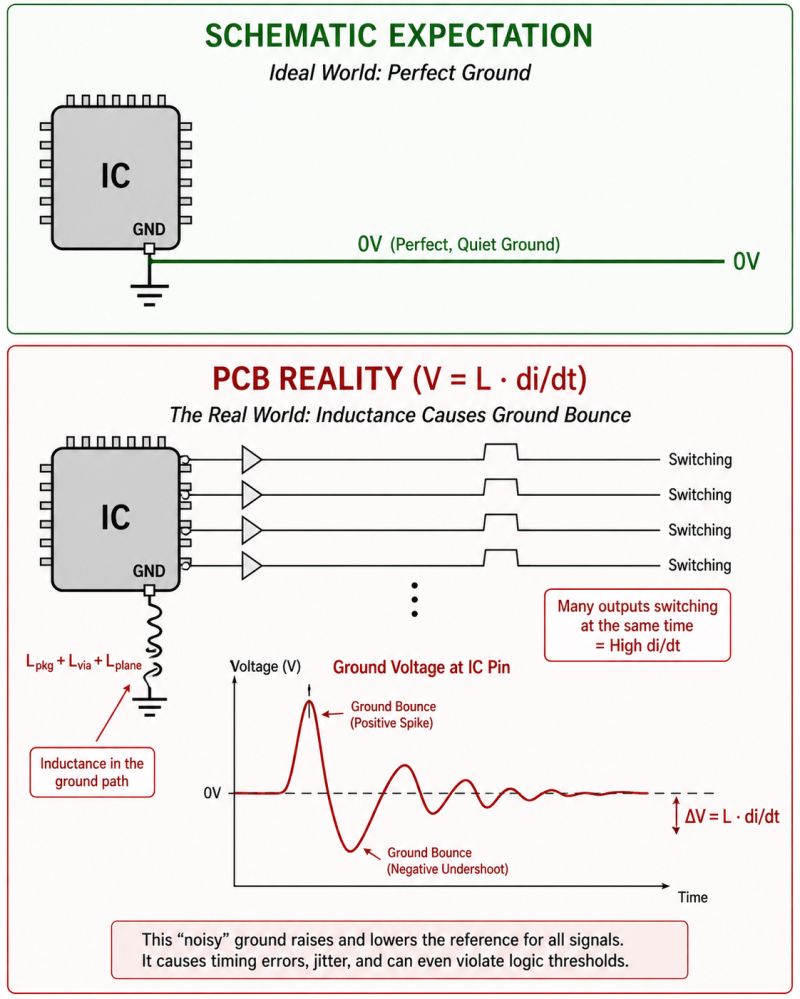
-->  Ground Bounce and the Myth of "Zero Volts" <-- Have you ever had a perfectly clean signal suddenly start failing, just because other signals on the board were switching at the same time? Welcome to the world of Simultaneous Switching Noise (SSN), also known as Ground Bounce. When we look at a schematic, we treat "Ground" as a magical, infinite sink that is perfectly at 0V everywhere. But in the physical high-speed world, Ground is just another piece of copper. And all copper has parasitic Inductance (L). When a digital chip drives a signal from High to Low, it rapidly dumps current into the ground return path. If you have an 8-bit or 16-bit data bus where multiple pins transition from High to Low at the same nanosecond, you get a massive, sudden surge of current (di/dt). Here is the only physics equation you need to understand why your board fails: V = L.(di/dt) Because the ground pin on your IC package and the vias connecting it to the PCB ground plane have inductance (L), that sudden spike in current (di/dt) creates a real voltage (V) across the ground connection. For a brief moment, the "Ground" inside your chip might bounce up to 0.5V or even 1V! To a receiver, this Ground Bounce looks exactly like a signal glitch. It can cause false logic triggering, double-clocking, and massive timing errors. How do we fix it? You can't easily change the di/dt (that’s your required clock speed and data rate). You MUST lower the Inductance (L). This means using multiple ground pins, placing components closer to the planes, and optimizing your decoupling capacitor mounting inductance! Have you ever battled Ground Bounce on a densely packed data bus? How did you solve it? Let me know below! 👇
RayPCB tweet media
English
0
35
242
14.1K
RayPCB
RayPCB@RaymingTech·
🔧 Just reviewed an Arduino Uno R3 clone PCB – and the engineering quality is impressive. This isn’t over-engineered. Every component serves a clear purpose, and the layout shows real attention to signal integrity, power distribution, and manufacturability. Standout features: ✅ Smart PCB layout – clean traces, isolated oscillator, centrally placed voltage regulators ✅ Robust power management – stable 5V/3.3V rails, filtering, reverse polarity protection, separated analog/digital domains ✅ Full I/O – 14 digital, 6 analog (10‑bit ADC), 6 PWM, USB serial up to 115200 bps ✅ Production‑ready – precise footprints, via stitching, gold‑plated connectors, clear silkscreen ✅ 100% Uno R3 compatible – true drop‑in replacement, no software changes What I appreciate most: It respects both the maker community and manufacturing realities. The design balances performance, cost, and reliability – exactly what you want in a microcontroller board. Perfect for: IoT prototyping, robotics, home automation, sensor networks, education, and industrial embedded systems. If you’re into embedded systems, PCB design, or hardware engineering – what’s your #1 priority when reviewing a board? Let’s discuss 👇 #Arduino #PCBDesign #EmbeddedSystems #IoT #HardwareDesign #EngineeringExcellence #Maker #Robotics
RayPCB tweet mediaRayPCB tweet mediaRayPCB tweet media
English
5
5
51
3.6K
RayPCB
RayPCB@RaymingTech·
SMD Soldering
English
0
3
40
1.7K
RayPCB
RayPCB@RaymingTech·
Two main ways data travels: Serial vs. Parallel – and why it still matters today. 🔹 Serial communication sends data one bit at a time over a single line. Fewer wires → simpler, lower cost, and more reliable over long distances. That’s why protocols like USB, UART, SPI, and I2C rely on it. 🔹 Parallel communication sends multiple bits at once across multiple lines. Faster over short distances, but more wires and risk of timing skew (bits arriving at different times). In practice: ✅ Serial wins for long-distance and most modern systems. ✅ Parallel is still used inside devices where high speed over short distance is needed (e.g., memory buses). Understanding these trade-offs helps you design smarter, more reliable systems. Which one do you use more often in your projects? 👇 #EmbeddedSystems #DataCommunication #HardwareDesign #ElectronicsEngineering
RayPCB tweet media
English
0
5
26
653
RayPCB
RayPCB@RaymingTech·
The principle of binary computation
English
0
1
9
645
RayPCB
RayPCB@RaymingTech·
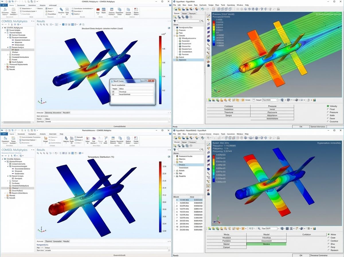
Why risk a costly prototype failure when you can simulate your way to success? The difference between a failed mission and a breakthrough flight often comes down to one thing: high-fidelity simulation. At Varun Dynamics, we give drone manufacturers a Digital Proving Ground—so you can perfect your design before cutting a single physical component. Check out our 4-point tactical analysis below 👇 🛡️ Structural Stress – Identify high-stress zones and ensure airframe integrity. 💨 Aerodynamic Flow – Visualize streamlines to maximize lift and extend battery range. 🔥 Thermal Mapping – Prevent mid-air failures with optimized motor and battery cooling. 🌀 Vibration Control – Eliminate resonance for rock-steady gimbals and sensors. The Varun Dynamics advantage: ✅ 15 IIT PhDs leading the way ✅ 45% faster development cycles ✅ AI-integrated geometry optimization (G-AI Core) From tactical loitering munitions to commercial delivery fleets—we engineer confidence behind every flight. 🚀 Ready to optimize? Let’s talk.
RayPCB tweet media
English
1
2
12
342
RayPCB
RayPCB@RaymingTech·
🚀 6-Layer PCB Design: The Stack-up & Via Strategy A successful high-speed PCB isn't routed; it's planned. Today, I focused on the critical foundation of board design using Altium Designer: Stack-up configuration and Via technology. 🔧 The 6-Layer Setup: Layers: 1, 2, 3, 5, 6 (Signals) | Layer 4 (GND) Note: Placing the ground plane close to the power plane helps decoupling and reduces high-frequency noise. 🔍 Via Technologies: Through-Hole: Standard connectivity. Blind/Buried: Essential for HDI designs to free up routing channels. Via-in-Pad: Crucial for BGA fan-out and minimizing parasitic inductance. 📚 Current Focus Areas: Signal/Power Integrity (SI/PI) Controlled Impedance & Differential Pairs DDR Memory Routing Concepts IPC Standards & DFM Designing for performance means designing for manufacturability. Every layer and via choice is a step toward a reliable, high-speed product. #PCBDesign #Altium #Engineering #TechLearning #HighSpeed #HardwareDesign
RayPCB tweet media
English
1
3
22
705
RayPCB
RayPCB@RaymingTech·
PCBA pin assembly soldering machine, automatic board loading machine, flipper, depaneling machine production line #Automation Equipment #RayPCB
English
0
0
3
148
RayPCB
RayPCB@RaymingTech·
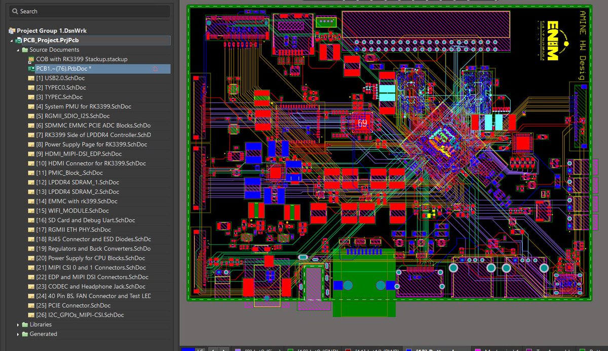
🚀 12-Layer High-Complexity Embedded Board Design (RK3399) I’m excited to share a recent hardware design project: a 12-layer PCB built around the RK3399 processor for high-performance embedded systems. This board integrates multiple high-speed interfaces and critical modules: 🖥️ Processor – RK3399 (ARM Cortex-A72 + Cortex-A53) 💾 Memory – LPDDR4 💽 Storage – eMMC 🌐 Networking – Ethernet (RGMII), Wi-Fi module 🔌 Interfaces – USB 2.0, HDMI, MIPI DSI, eDP, PCIe, SD card 🎧 Audio – Codec + headphone output 🧠 PCB Stackup & Architecture 12 layers with dedicated GND and power planes Internal layers optimized for high-speed routing Stackup designed for signal integrity, power integrity, and EMI/EMC reduction ⚙️ Key Technical Details High-speed routing Length matching for LPDDR4 and critical buses Differential pair management (USB, HDMI, PCIe) Impedance control – 50Ω single-ended / 90Ω differential Power & ground planes Continuous ground plane to minimize noise Segmented power planes by domain Stitching vias to improve current return paths Component placement Optimized placement around the CPU Reduced critical lengths (DDR, clock signals) Clean separation of analog and digital zones Power supply Switching buck converters Multi-domain distribution (CPU, DDR, I/O) Optimized decoupling network 🛠️ Tools & Methodology Altium Designer – schematic & PCB layout Advanced design rules (DRC) Constraints: length matching, differential pairs, controlled impedance 3D PCB visualization for validation 📊 Results ✅ High-density PCB realized ✅ Complex high-frequency signals integrated ✅ Stable architecture for advanced embedded systems ✅ Compliant with industrial design constraints 📌 Conclusion This project marks a major step forward in my hardware design journey — especially in the areas of multilayer PCBs and high-performance embedded systems. I’d love to hear your thoughts or connect with fellow hardware engineers working on similar challenges. Let’s discuss! 🔧
RayPCB tweet mediaRayPCB tweet mediaRayPCB tweet mediaRayPCB tweet media
English
0
3
11
426
RayPCB
RayPCB@RaymingTech·
FM in Practice #7 | The Ultimate PCB Layout Survival Guide: 50 Pitfalls to Avoid Most engineers think PCB layout is just connecting dots. In reality, a bad layout isn't a small mistake—it's the fastest way to crash an entire hardware project. The hidden physics of routing 🛠️ You're not just drawing lines. You're managing impedance, return paths, EMI, and layer stackups—all at once. Routing "wherever there's space" guarantees signal collapse. High-frequency design needs precision, not just connectivity. The "via tax" on signals 📉 Vias aren't free. In high-speed designs, every extra via is a parasitic tax on your signal. More vias = more distortion and loss. If you're not calculating via transitions, you're guessing, not designing. Placement over quantity ⚖️ Decoupling capacitors? Placement beats quantity every time. A hundred caps in the wrong spot won't suppress power noise as well as one cap placed correctly. It's about proximity to the pin, not the BOM count. Analog vs. digital: the great divide 🏗️ Partitioning analog and digital zones is more critical than most realize. It's not just organization—it's the logic that solves systemic interference. Cross that line, and you'll chase noise for weeks. EMI is built in, not patched out 🛡️ EMI suppression isn't an afterthought. It must be baked into your layout and stackup from day one. Prevention at the CAD stage is 100x cheaper than a respin after a failed lab test. The eCloud Survival Guide ☁️ At eCloud Technology Co., Ltd., we've reviewed thousands of designs. We've compiled the 50 Most Common Layout Pitfalls—the ones that trip up everyone from juniors to senior RDs. Most hardware failures aren't discovered during debugging. They're decided the moment you finish the layout. Don't let yours be one of them. 👉 Save this post – and follow for more FM in Practice.
RayPCB tweet media
English
2
4
30
1.3K
RayPCB
RayPCB@RaymingTech·
SMT Reflow Soldering
English
1
2
33
3.2K
RayPCB
RayPCB@RaymingTech·
PCB Drilling
Dansk
1
1
21
955
RayPCB
RayPCB@RaymingTech·
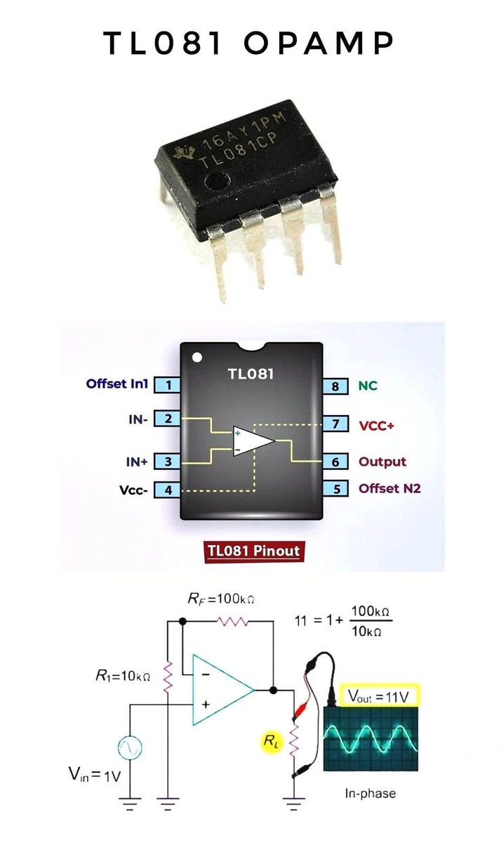
Understanding the TL081 Op-Amp in a Non-Inverting Amplifier Configuration 🔧 The TL081 is a classic JFET-input operational amplifier valued for its high input impedance and low noise—ideal for signal amplification in audio, sensor, and conditioning circuits. Here’s a quick pin breakdown: Pin 3 → Non-inverting input Pin 2 → Inverting input Pin 6 → Output Pins 7 & 4 → Positive & negative supply Pins 1 & 5 → Offset null adjustment Pin 8 → Not connected In a non-inverting amplifier configuration, the input signal goes to the positive terminal (pin 3). The gain is set by two resistors: Gain = 1 + (Rf / R1) With Rf = 100kΩ and R1 = 10kΩ → Gain = 11 So a 1V input produces an 11V output—same shape, same phase, no inversion. That makes the TL081 a go-to choice when you need clean, in-phase amplification. 💡 Have you used the TL081 in any of your designs? Share your experience below! #OpAmp #ElectronicsEngineering #SignalProcessing #CircuitDesign #TL081
RayPCB tweet media
English
0
11
87
2.1K
RayPCB
RayPCB@RaymingTech·
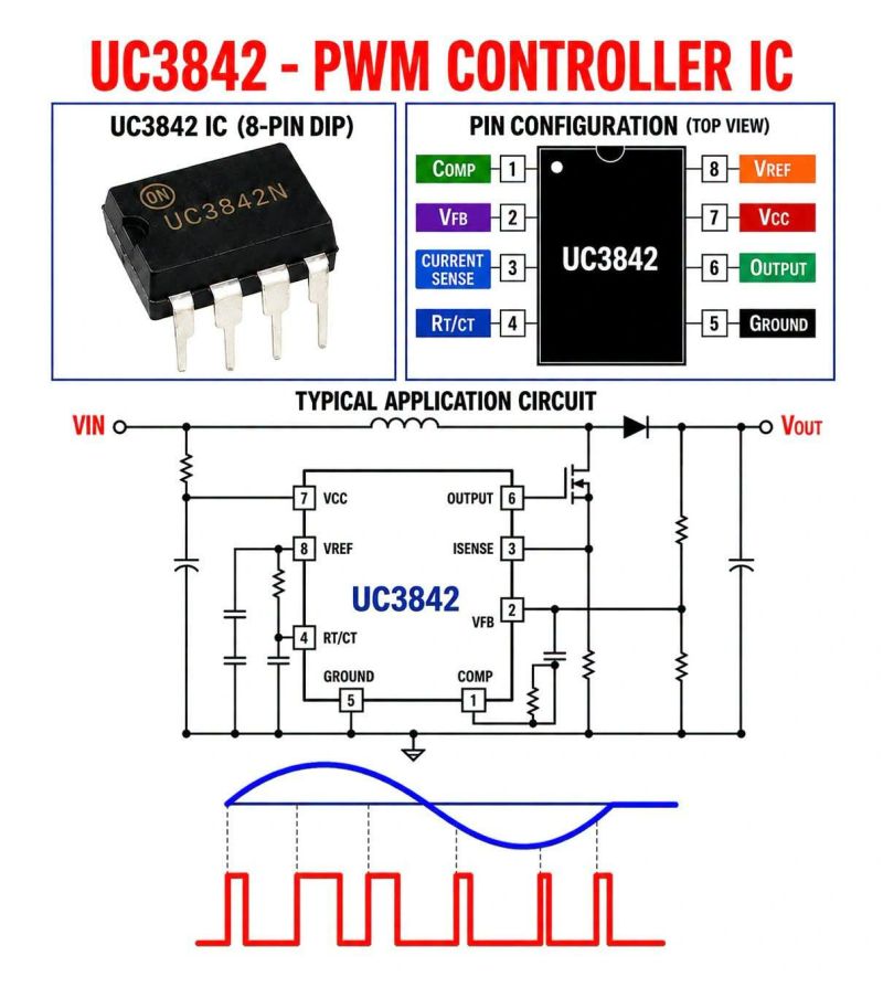
The UC3842 is a popular PWM controller IC used in SMPS, DC-DC converters, battery chargers, and LED drivers. It regulates the output voltage by controlling the switching of a power MOSFET using Pulse Width Modulation (PWM). The feedback pin keeps the output stable, while the current-sense pin provides overcurrent protection. The oscillator sets the switching frequency, making the converter efficient and reliable. Its built-in protection and simple design make the UC3842 a widely used IC in modern power electronics.
RayPCB tweet media
English
1
21
155
4.2K