Harn bos
1.1K posts


@pauluscremers Jaman denk het wel. Ze zeggen dat ze chips op elkaar gaan stapelen alleen zeggen niet hoe….
Nederlands
@Salehaldin0b Waarschijnlijk iets dat TSMC over hybrid bonding gezegd heeft.
Nederlands

@pauluscremers Waarschijnlijk iets dat TSMC over hybrid bonding gezegd heeft.
Nederlands


$SPY top could be ATH or it could lower high but I got this date mathematically calculated to be the most significant: July 2026.
The actual date is in the thread.
This is one of my profound studies I've ever done.
Jay Gann 📈📉🗓 | CIT Change in Trend Dates@TradesJayGann
"The 12H Extraction Protocol" The "Air" regime is leaking. The narrative is dissolving. I’ve spent the last 72 hours mapping the 2007 GFC fractal against the current 2026 cycle. What I found isn't just a "pullback"—it’s a structural uprooting. The 12H Extraction has begun 🧵👇
English
@ArendJanKamp Als jij hebt gekocht weet ik in ieder geval dat hij morgen naar beneden gaat.
Nederlands

De allerlaatste dan van mij over cijfers #ASML morgen... dat wij gisteren al voor de #StockWatch Big Data Porto kochten
Hoe, wat en waarom?
Zie onze YouTube video youtube.com/watch?v=UwPdyj…

YouTube
Nederlands
@pauluscremers @jukan05 Ik had mij er vorige keer op verkeken, dat dit ook nog eens precies in beide gevallen 11 dagen na earnings is gebeurt…. Manipulatie pur sang. Ik ga kijken of dit soort dingen vaker voorkomen. Kijken of ik hier kan inspelen.
Nederlands

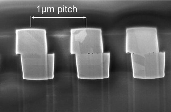
Next-Gen HBM Thickness Relaxation Gains Momentum… A Blow to Hybrid Bonding
Major semiconductor companies are reportedly in discussions to relax the thickness standard for next-generation high-bandwidth memory (HBM), which requires 20-layer stacking. Figures ranging from 825 to 900 micrometers (μm) and above are being floated — surpassing the 775μm thickness of HBM4 (6th-generation HBM), which is set for full commercialization this year.
According to ZDNet Korea's reporting as of the 6th, participants in JEDEC (the Joint Electron Device Engineering Council) are actively discussing a significant relaxation of thickness standards for next-generation HBM.
Next-Gen HBM Thickness Standard: Discussions Reach 825–900μm and Beyond
HBM is a next-generation memory built by vertically stacking multiple DRAM dies and connecting them via microscopic bumps. Through HBM3E, the thickness standard had been held at 720μm, but it was raised to 775μm with HBM4, largely due to the increased stack count of 12 and 16 layers — up from 8 and 12 in the previous generation.
Now, the industry is discussing further relaxation of thickness standards for next-generation HBM — namely HBM4E and HBM5 — which will stack DRAM in 20 layers. The figures currently under discussion range from 825μm to over 900μm. Should the standard be set above 900μm, the increase would substantially exceed any prior jump.
"JEDEC needs to finalize key standards one to one-and-a-half years before a product reaches commercialization, so discussions around next-gen HBM thickness are very active right now," said one semiconductor industry official. "Figures above 900μm are already being thrown around."
JEDEC is the international standards body for semiconductor products. Its membership includes memory companies such as Samsung Electronics, SK Hynix, and Micron, as well as major global semiconductor firms including Intel, TSMC, NVIDIA, and AMD.
Historically, the industry has been extremely strict about limiting HBM thickness increases. If HBM were allowed to grow thicker without constraint, it would become increasingly difficult to match the thickness of system semiconductors — such as GPUs — that are integrated horizontally alongside it. Excessive spacing between DRAM layers also lengthens data transmission paths, degrading performance and efficiency.
As a result, memory companies have pursued a range of technologies to keep HBM thin, most notably thinning processes that grind down the backside of core DRAM dies, and bonding technologies that reduce inter-die spacing.
Both Memory and Foundry Players Want Thickness Relaxation
Despite these efforts, there are two primary reasons why the industry is now actively discussing relaxing the thickness standard for next-generation HBM.
The first is the shift to 20-layer stacking. Existing thinning processes and inter-die bonding technologies are approaching their limits in terms of how thin HBM can realistically be made.
The packaging roadmap of TSMC, a leading foundry, is also a contributing factor. TSMC currently holds a near-monopoly on 2.5D packaging (CoWoS), which integrates HBM and GPUs into a single AI accelerator. CoWoS uses a wide interposer inserted between the chip and substrate to enhance packaging performance.
TSMC's next step beyond 2.5D packaging is SoIC (System-on-Integrated Chips), which vertically stacks system semiconductors at extremely fine pitch in a true 3D configuration. In AI accelerator applications, TSMC-SoIC would combine the stacked system semiconductor with HBM.
When TSMC-SoIC is applied, the thickness of the system semiconductor increases by tens of micrometers or more beyond the current 775μm baseline — making a corresponding relaxation of HBM thickness standards essentially inevitable. NVIDIA and Amazon Web Services (AWS) are among the companies reportedly planning to adopt TSMC-SoIC.
"The need for next-gen HBM thickness relaxation isn't coming from memory suppliers alone — foundry players have a stake in it too," said one industry official. "It's too early to say definitively whether it will be adopted, but discussions are clearly happening among major players."
Industry: "Demand for Hybrid Bonding Could Decline"
Industry observers interpret these discussions as a factor that could slow the adoption of next-generation bonding processes such as hybrid bonding. Bonding refers to the process of joining individual DRAM dies within an HBM stack; currently, the dominant method is TC (thermocompression) bonding, which uses heat and pressure.
Hybrid bonding directly joins the copper interconnects of chips and wafers, eliminating the bumps between DRAM layers and effectively reducing inter-die spacing to near zero — making it highly advantageous for reducing overall HBM package thickness.
However, hybrid bonding is technically extremely challenging. It requires: complete removal of microscopic surface contaminants to achieve seamless chip-to-chip bonding; CMP (chemical mechanical planarization) to achieve a perfectly smooth chip surface; and high alignment precision to ensure accurate mating of each copper pad. Yield can also drop sharply when bonding all 20 dies in sequence.
As a result, while major memory companies have continued to research and develop hybrid bonding, none have yet applied it in mass production of HBM. Even Samsung Electronics — the most aggressive developer of hybrid bonding — is only expected to incorporate the technology partially, and at the earliest in HBM4E 16-layer configurations.
In this context, if next-gen HBM thickness standards are relaxed, memory companies are likely to continue mass-producing HBM using TC bonders.
"There's a view in the industry that even a 50μm relaxation in HBM thickness would be sufficient to enable 20-layer stacking," said one industry official. "And since introducing hybrid bonding would require full replacement of existing equipment at enormous cost, my understanding is that memory companies are broadly in favor of relaxing the next-gen HBM thickness standard."
English
@scetrader Ja Shell en Besi short dan heb je wel een mooie hedge. Ik zeg maar wat tho. Heb zelf net een Besi put gehaald. 😂👍
Ja in een markt als deze kun je beter iets voorzichtiger zijn idd.
Nederlands

🎉 Wall Street bias: Welke optie combinatie is het beste voor vandaag #0dte $SPX $ES $SPY $NDX $NQ $QQQ
scetrader.nl/wall-street-bi…
Nederlands
@bos_harn They preannounced 4Q, 10 days into January maybe will do same with Q1?
English
@scetrader Je hebt gelijk alleen je kunt het er zeker wel in lezen.
Nederlands
Die gast is niet goed hoor. Wat een onzin. Voor alle duidelijkheid: hij heeft tijdelijk bij de eerste termijn van Trump in het Witte Huis gewerkt en met ruzie vetrokken.
Anthony Scaramucci@Scaramucci
Wake up: he is calling for A NUCLEAR STRIKE. Seek his removal immediately.
Nederlands
@Salehaldin0b Who knows, maybe. But last weeks news about the SK Hynix order for Amat & Besi does imply at least solid earnings later in April. 👌
English
$SPY Purple Gann Angle 3x1 is a good area for resistance. IYKYK

English

@scetrader Ja eens ik snap wat je bedoelt, maar je kunt het vermoorden van mensen nooit goedpraten. Je kunt niet zeggen van o daar zit een organisatie die wij terroristen vinden dus dat geeft ons het vrijrecht om iedereen met diezelfde gedachtegang te vermoorden vind ik.
Nederlands
Waar het om gaat, is dat het nieuws zoals het wordt gebracht niet klopt. Door dit soort berichtgeving kan antisemitisme weer verder toenemen. Daarnaast is het moeilijk te begrijpen waarom een terroristische organisatie, die in de meeste westerse landen ook als zodanig wordt aangemerkt, de hand boven het hoofd wordt gehouen.
Nederlands
Wat een gotspe. De NOS brengt een item waarin Israël wordt beschuldigd van het doden van drie journalisten in Libanon. Bij de begrafenis zijn allemaal vlaggen van Hezbollah zichtbaar, maar nee, het zouden journalisten zijn. Nee, dit zijn terroristen vermomd als journalisten. De NOS gaat steeds verder in haar propaganda. Wat ze er namelijk ook niet bij vertellen is dat Libanon aan Israel heeft gevraagd voor hulp tegen Hezbollah, dat een proxy is van het regime in Iran. Wat er ook niet bij wordt verteld, is dat Noord-Israël onder een constante regen van raketten van Hezbollah ligt. Het heeft niets met de handel te maken, maar dit moest even gezegd worden.
Nederlands