
Sabitlenmiş Tweet
얀도링
11.2K posts

얀도링
@dara8887
- 헛소리 많으므로 팔로비추 (님들의 탐라가 쓰잘데없는 소리로 가득찰겁니다)
Katılım Ocak 2025
254 Takip Edilen54 Takipçiler
본인들이 무슨 정의의 사도라도 된 것마냥 행세하고 있는데,
본인들이 담화 맥락을
"물화는 이과의 근본 과목이므로 모든 이과계 사람들은 고등학교 물화를 수강해야 하며, 수강하지 않은 사람은 이과계 학과를 갈 '자격'이 없다. 그 사람은 애초부터 '이과 체질'이 아닌거다."
라고 잡고 있는게 얼마나 무지하고 편협한 말인지 이해를 못하는 것인지? 이게 이해가 안돼? 내가 맥락맹이라고 주장을 하는데, 아니... 본인들이 한 말을 돌아보라니까?
본인들이 정말로 순수하게 학종 이야기를 하고 있는 건지, 얼토당토 않은 엘리티시즘에 빠져있는건지 생각해보라고.
너네 선동하고 있는거야 지금
얀도링@dara8887
한국어
[소신]
고등학교 물화 별거아니니까 그냥 대학 들어가서 배워도됨
일물 일화 전공기초로 가르쳐주잖아
뭔 특별한거 배우는줄
별거아님 쫄지마
뭔 중학교 내신을 잘따려면 미리미리 구몬 학습지를 해둬야해요 ㄷㄷ 보는것같네
໊@lifroab
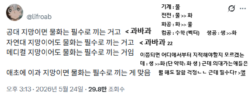
공대 지망이면 물화는 필수로 끼는 거고 자연대 지망이어도 물화는 필수로 끼는 거고 메디컬 지망이어도 물화는 필수로 끼는 거임 애초에 이과 지망이면 물화는 필수로 끼는 게 맞음
한국어
"물리 화학 안하면 이과 체질이 아니다, 이과 갈 생각도 하지 마라."
이런 유언비어를 퍼트리고있는데 이걸 어떻게 그냥 내버려둠? 그렇지 않더라도 이과계에 적성이 없는게 아닐 수 있다고.
그리고 스스로 위와 같이 주장했으면서 어떤 염치로
"나는 학종 이야기만 한거다" 라고 뒤늦게 포장함?
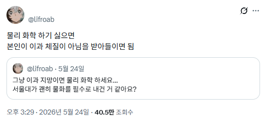
໊@lifroab
내 말은 이거였지 라고 할 거면 트윗을 내리는 게 좋지 않을까요? 늙크크 + 맥락맹이신 걸 남의 트윗 위에 글까지 써 가면서 티내실 필요는 없어 보이는데
한국어
@LL58919051131 안녕하세요, 답변 드리기 이전에 한 말씀 여쭙고 싶은데, (비꼬려는게 아니라 정말 몰라서 드리는 질문입니다) 물화 선택 하지 않으면 아예 모든 학교가 안뽑아주는건가요?
한국어

현직 중, 고등학교 멘토링 담당입니다.
좆도 안 되는 개소리 집어치우십쇼.
뭔 저런 무책임한 이야기를 하고 있어...
얀도링@dara8887
[소신] 고등학교 물화 별거아니니까 그냥 대학 들어가서 배워도됨 일물 일화 전공기초로 가르쳐주잖아 뭔 특별한거 배우는줄 별거아님 쫄지마 뭔 중학교 내신을 잘따려면 미리미리 구몬 학습지를 해둬야해요 ㄷㄷ 보는것같네
한국어
본인 발언 돌이켜 생각하고 말하시길...
입시 이야기인 것을 몰랐음은 타래에 정정했음.
따라서 인용의 입시생들의 억울함 토로는 정당함. 하지만 당신은 아님.
내가 반박하고자 한 것은 뭔 고등학교 물리 화학을 '과학' 인 것마냥 주장하는 것이 우습다는 소리였다.
'입시'가 아니라 '과학'을 논하려거든,
최소한 과학 계통에 소속되어 있기를 바람.
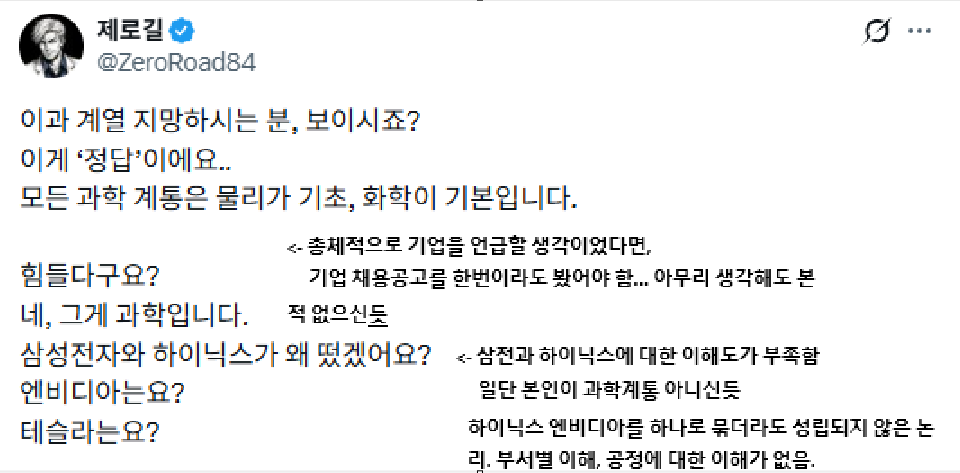
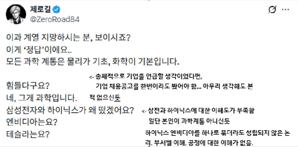
제로길@ZeroRoad84
신박한 소신 발언 접어두시죠. 물리 화학 배우고 못 배우고 얘기가 아닙니다. 대학에서 선택과목으로 물리 화학을 해야 좋은 평가를 받는다는 겁니다. 중학교 내신 따겠다고 구몬하냐는 신박한 소리는, 본인이 지금 하고 있는 말이에요.
한국어
@nyang20258 튜링님도 섀넌님도 수학자였지.. 노이만님은 물리학자로 보기에는 너무 올라운더인데다가, 당장에 스승이 힐베르트님이라네여... 노이만 구조 레포트 보면 아시겠지만 물리학적 배경은 전혀 없고요... 그 논거라면 오히려 수학을 알아야 한다는 쪽이 더 맞겠네요... 아무튼 대화 재미있었습니다...
한국어

말씀하신대로 꼭 필요하지는 않은데 기초적인 물리화학적 관점? 정도는 중요하죠.
특히 컴공은 물리 좀 알아야해요 ㅠㅠ 다 그쪽 사람들이 만든거라
대기업 면접 같은데서도 간단한 역학문제 정도는 나오기도 하고 그래요!
근데 저도 그걸 꼭 시험을 봐야하냐? 하고 묻는다면 그 정도 수련을 해야하는지는 의문이 있습니다.
한국어
원론적으로 대체 어케 맞습니까....
컴공가서 물화 쓰실일 있으셧는지? ... 전 수학밖에 쓴 기억이없음...
전전가서는 반도체 배울때 화학 정말 한 스푼 (Si 구조 설명 용도) 정도만 봤었고, (되려 순수 물리+수학),
기계 가서 화학은 본 적이 단 한번도 없고,
화공도 화학 베이스에 물리 한 티스푼 넣어 가르치는데 원론적으로 대체 뭐가 맞는지?.........
화학 써먹을거면 애초에 이온 위주로 문제내지 말아야지... 배터리할건지? 물리(역학) 써먹는 과목도 사실 적습니다... 혹시 다른 학과 수업이나 커리큘럼을 본 적은 있으신지요?.....
한국어
@dara8887 ㅋㅋㅋㅋㅋ 아 오른쪽 한분은 선생님이시더라구요 ㅋㅋ 문과쪽이신거같아요.
아무래도 마음은 좋은 분 같은데 옛날분 느낌이 없진 않은 정도?
왼쪽도 원론적으로는 맞긴 맞으니 ㅋㅋㅋㅋ
정밀하게 입시에 대해 따지면 또 다르지만요...
한국어
얀도링 retweetledi

낸드(NAND) 발명자는 일본 도시바(Toshiba)에서 근무하던 마스오카 후지오(舛岡富士雄) 박사입니다. 그는 전원이 꺼져도 데이터가 지워지지 않는 플래시 메모리를 발명(1980년)한 이후, 1986년에 현재 대용량 저장 장치에 널리 쓰이는 낸드(NAND) 플래시 메모리 구조를 고안했습니다. 그런데 사업 성공 후에도 보잘것 없는 보상에 놀랐습니다. 일본도 한국과 다를 바가 없었네요.
ひろ🐼データをストーリーで語るマーケター@hiro_panketing
キオクシア(旧東芝メモリ)の2026年売上は2.3兆円。 この会社の屋台骨を作った発明者が、東芝から受け取った対価は、8,700万円やった。 異常やった。 舛岡富士雄さん。 スマホ・SSD・USBメモリ、全部に入ってる「NAND型フラッシュメモリ」の発明者。 1987年に東芝で作り上げた技術が、40年後に世界を変えた。 でも発明した後、東芝社内で何が起きたか。 擁護してくれた上司が1991年に急逝。 翌年、提示されたポストは「研究所付技監」。 肩書きはあるけど、部下なし・研究費なし。 舛岡さんはこう言ってる。 「研究の場を失うのは、エンジニアにとって死を意味します」 3年間抵抗したけど、1994年に東芝を去った。 その後、2004年に「せめて40億円は認めてほしい」と提訴。 2006年に和解が成立して、受け取った額が8,700万円。 要求額のたった2%。 その間、東芝は舛岡さんの発明で生まれた特許を、インテルに二束三文で売り払った。 2.3兆円の売上を生む会社を作った発明が、8,700万円で終わった。 日本の企業が「天才を閑職に追いやる」と何を失うか、この数字が全部言ってる。 発明の価値は、会社が決めるもんやない。
한국어

@nyang20258 캣님은 정말 마음이 넓고 온화하신 분이군요..... 이런마음가짐을 나도 가져야 하는데.... 본받겠습니다... 원트의 대범한 발언에 어그로가 끌리고만 나머지 회의적인 시선만 가지게 되었었네요...
한국어
@dara8887 꿈은 뭐 자유니까요 ㅎㅎ 매해 입학 정원이 그정도면 고3들만 보는 것도 아닐거고, 그냥 심심해서 보는 사람도 사실 많을거구요
한국어
@alice_in_noel_ @SVTrivo 이게 당장에는 맞는 방향처럼 보이는 것 같습니다... 사람들이 생태계 위에서 하드웨어 만지작만지작하면서 어디까지 되고, 어디에서 효율이 좋고, 어느 어플리케이션에 적합한지 탐색하는 과정이 필요한 듯 한데, 역시 생태계 진입이 가장 큰 관건이 될지도 모르겠습니다... 신기하네요...
한국어

다좋은데 44GB 너무 작지 않나? ...
큰 모델 위해 어차피 DRAM 연결해 쓸거면 SRAM으로 가득채운 의미가 많이 희석되지 않나 싶다....
그렇다고 더 작은 모델 넣기에는 성능이 충분할까? 라는 의문이 들어....
극복 위한 알고리즘이 있다는건가? 아니면 중간 모델 쯤에서 속도로 승부보겠다?
Papa Johns@SVTrivo
Cerebras's insane yield strategy: One perfect giant chip vs. a flexible swarm of many small cores Imagine a flagship smartphone AP chip. It packs dozens of CPU cores, a powerful GPU, NPU, 5G modem, image processor, audio DSP, Bluetooth, security engine — everything in one big die. If even a single block has a defect during manufacturing — calls keep dropping, audio crackles, or the camera glitches — the entire chip is thrown away. That's the harsh reality of traditional large-chip yields. Every single function must be 100% perfect to pass. As dies get bigger, defect probability skyrockets. In cutting-edge 3nm or 2nm processes, hitting even 50-60% yield is considered a big win for mass production. Cerebras $CBRS completely flipped this rule. They take an entire 300mm wafer and turn it into one massive chip (the WSE-3). Inside are 970,000 tiny AI cores, all identical, each about 0.05mm². They operate independently and connect through a smart switch network. The key difference is how they define a good chip: "90,000+ working cores = Pass" - Defective cores are automatically bypassed. - Surrounding wiring simply acts as pass-through fabric. - Only the SRAM attached to the surviving cores is used. The result? 93% silicon utilization. They receive the whole wafer, carve 44GB of on-chip SRAM into 970,000 pieces, and use only what's attached to the 900,000+ good cores. The bad parts? Just discard them. The cost is already baked into the full-wafer price anyway. While traditional chip companies struggle to push yields past 60% on advanced nodes, Cerebras already achieves over 93% on a full wafer. This isn't a simple trick. It's a fundamental paradigm shift. - Traditional approach: Chase one perfect large die → extremely vulnerable to defects - Cerebras approach: Connect many slightly imperfect small cores → tolerate defects while delivering extreme performance Thanks to this, Cerebras can build AI inference chips that compete directly with Nvidia, without suffering the usual yield headaches. Of course it's incredibly hard to copy. It required a decade of work on dynamic routing for hundreds of thousands of cores, full-wafer testing, custom software stacks, and deep foundry partnerships. But the outcome is clear: Cerebras has become one of the few companies to overcome yield limits through architecture. And that crazy originality is now heading to the public market through their IPO. x.com/SVTrivo/status…
한국어

@dara8887 추론용으로 특화되어 운용할 듯 합니다.
90만개의 코어로부터 외부 DRAM이나 HBM 연결은 장점을 죽이는 일입니다.
학습용이나 기타 범용은 여전히 엔비디아 GPU의 영역입니다
Seven Trees, CA 🇺🇸 한국어