Noelia Solange retweetledi

Noelia Solange
409 posts

@noeliascotti
Electronics Engineer - PCB Designer
I have said this before, and I will say it again, because of the algo, not all posts reach all followers. I am a PCB designer, not an electrical engineer. Lots of people think I am an EE. I work with lots of EE to turn their schematic into a real object that works.

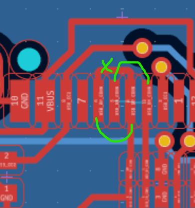
@noeliascotti @blind_via Here you go. Follows Wan-Hoorfar 2000 improvement on Svacina 1992's base paper.
🇦🇷 | NO LE DA LA CABEZA: El poco inteligente periodista de LN, Carlos Pagni, aseguró que el gobierno de Javier Milei comenzó en enero de 2023 y usó ese dato erróneo para argumentar que el salario real cayó cuando en realidad subió si se hace la comparación correcta con diciembre de 2023.
That looks like a fun trick. Staggering the pins on the header PCB footprint, so that you can insert the connector and make contact without soldering.
JLCPCBのPCB AでBGA使ったら5枚中2枚不良orz 顕微鏡画像がこちらでございます。 浮いてるわーorz

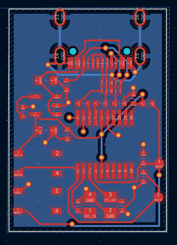
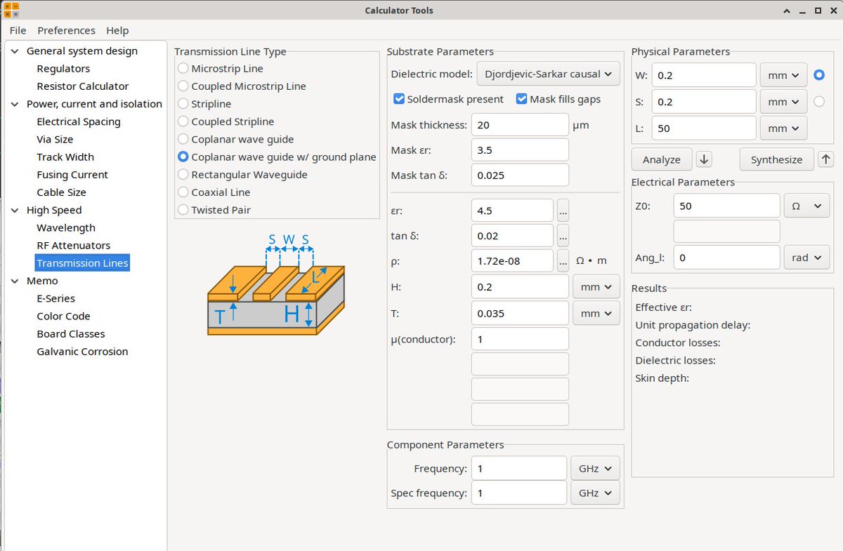
Impedance calculation will vary slightly depending on what calculator you are using to determine your trace thicknesses. Famously, PCB designers can get Saturn PCB ToolKit that has an impedance calculator. However, the Fabricators mostly use paid software called Polar. And the results you get between the 2 vary enough to cause issues with the fabricator accepting your impedance calculations. This is why it's a good reason to check with your intended fabrication house before committing to trace thicknesses in your complex design for controlled impedance. KiCAD has its own calculator, but it does not cover asymmetric stack up calculations at all, so I can't use it for those kinds of impedances calculations.

Dear PCB AI tool creators that keep asking me what I think about your tool. There are too many of you for me to commit meaningful time to this request. Make it worth my time, and I will make the time faster.