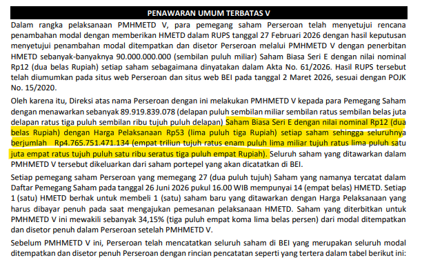
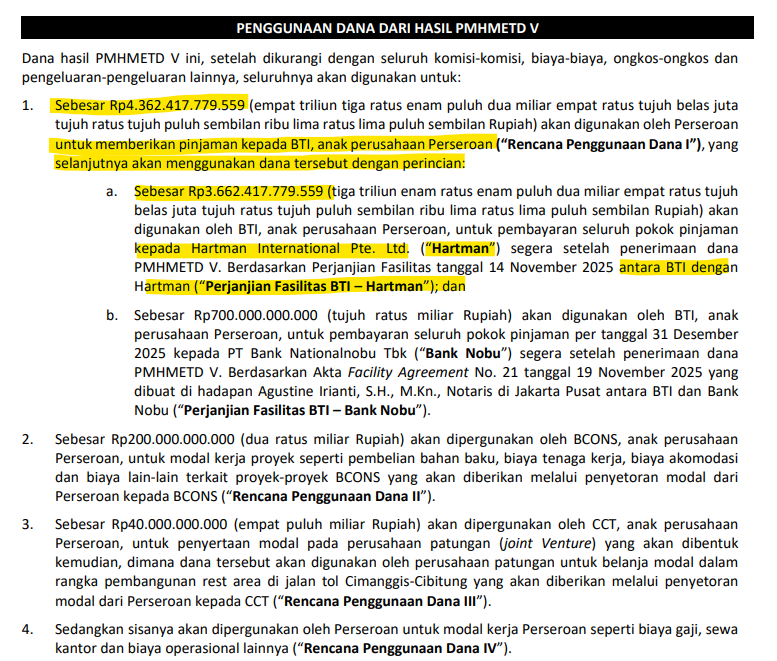
@ArvinHonami ga yakin klo itu buat bayar hutang , secara salim ada di ekosistem bakrie jd penasaran kungfu apa yang lagi di persiapkan😆
Indonesia
gnoisehch
126 posts


after 21 you actually need to stop eating indomie you too old for this


📍
Bryan Johnson breaks down his morning routine: 111 pills and 3 meals before noon "First thing I'll do is drink the Green Giant, take 60 pills, work out for an hour, eat Super Veggie, wait an hour, eat nutty pudding, wait one more hour, eat my third meal and I'm finished for the day" Steven: "How many pills do you take in one day?" Bryan: "Currently 111"

ANJIRR GA KEBAYANG ginjalnya si rey dipaksa grinding segitunya 😭😭😭11 suplemen langsung gas sekali telen, minumnya aja kagak proper, ya kalo emang mau fast track alam lain silahkan aja. Lucunya udah ada dokter nge stitch ngasih warning bahaya konsumsi suplemen barbar begitu, malah dokternya diblock 😭 influencer boti bego bikin konten ngawur kek gini tapi fans garis kerasnya di TikTok banyak banget njir


5 provinsi mati lampu Aceh, sumut,riau,sumbar,Jambi #Sumateragelap

Purbaya Yakin IHSG Lari Kencang Pekan Depan: "Saya pikir sih, kalau lihat dari teknikalnya sih, minggu depan udah lari kencang."
Sumatera Utara, sumatera Barat dan Riau malam ini blackout #Sumateramatilampu

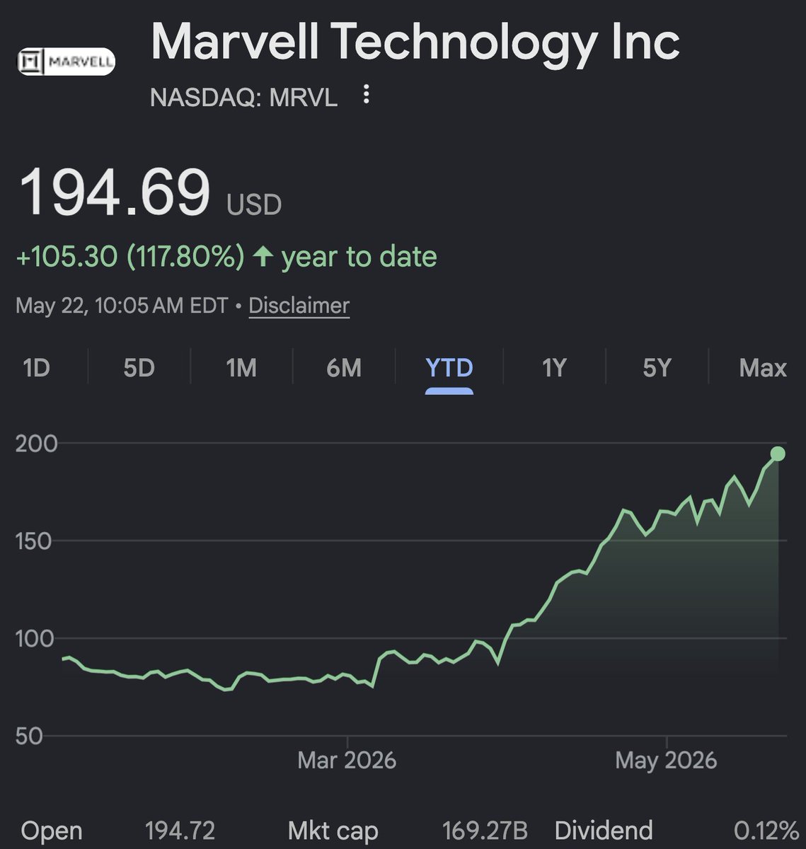
@MacnBTC Depends how long it takes retail to realize that there is a 15% dilution proposal coming up mid june. lol
Breaking the "Memory Wall": Optical Interconnects Emerge in GPU–HBM Packaging As a solution to the "memory wall," one of the chronic challenges in AI semiconductors, the memory and packaging industries at home and abroad are weighing an approach that decouples the GPU and high-bandwidth memory (HBM) and packages them separately. The core idea is to move the HBM—until now mounted right next to the GPU—a certain distance away, and bridge the gap with light (optics), allowing several times more HBM to be installed than is possible today. On the 22nd, a researcher at a major domestic memory maker said, "We're currently struggling to expand HBM bandwidth and capacity, so we're discussing with customers a plan to overcome the GPU's shoreline limit through optical interconnects and mount more HBM." Shoreline refers to the length of the chip's perimeter. In today's AI computing environment, the key factor dragging down compute efficiency is the data transfer speed of memory chips. While GPU performance has grown by leaps and bounds with each generation, the speed at which memory stores and supplies data has failed to keep pace—creating a structural performance barrier, the memory wall. The arrival of HBM, with its wide data pathways, put out the immediate fire, but critics continue to point out that bandwidth and transfer speeds still fall short of handling the explosive growth in AI compute. Until now, the industry has focused on stacking HBM ever higher to increase memory capacity and bandwidth within a confined footprint. But as stack counts climbed past 12 and 16 layers toward 20 and beyond, process difficulty rose exponentially. The technology hit physical limits, including the growing difficulty of meeting fixed height specifications. Vertical stacking has reached an inflection point—so much so that the JEDEC standards body has relaxed its HBM height specifications. The bigger problem is that if stack counts can't be raised, the alternative is to add more HBM horizontally around the GPU—but that, too, is impossible. In the current 2.5D packaging structure, the GPU and HBM are mounted tightly together on a single substrate. Within this structure, the number of HBM units that can be placed is strictly limited by the finite length of the GPU chip's perimeter—its shoreline. Even when more HBM is desired, there is physically no room to place it, leaving the industry in a structural deadlock. The alternative now emerging across the semiconductor industry is to separate the GPU and HBM and package them independently. It overturns the conventional chip-design principle that components must sit close together to minimize data transfer time. Instead of keeping the two chips adjacent, the approach spaces them apart and links them with overwhelmingly fast optical signals to overcome the added physical distance. Placing the HBM slightly away from the GPU within the board frees the design from the GPU's shoreline constraint. With the spatial limitation gone, far more HBM can be spread out laterally and packed into the board—several times more than today—without having to push stack heights to extremes. This means the total memory capacity and data bandwidth of the AI accelerator system would expand dramatically, on a scale incomparable to current systems. "Discussing Placing HBM Beneath the GPU"… Form Factor Could Change The industry is now producing a range of architectural design proposals over where exactly to place the HBM within the GPU board. The same memory researcher said, "Options under discussion range from broadly utilizing the space immediately around the GPU to isolating the HBM beneath the GPU board." He added, "In the latter case—isolating it beneath the GPU board—the motherboard would have to be extended lengthwise, so we're discussing even an overall form-factor change with the GPU maker." Specifically, the HBM might surround the GPU from several centimeters away, or a separate HBM zone might be created in the center of the board. "We're keeping every possibility open as we discuss the optimal layout," he said. "Nothing has been confirmed as an official roadmap yet, but as part of preliminary research toward next-generation AI accelerators, we're in talks with our partners." The outsourced semiconductor assembly and test (OSAT) industry is also watching this trend closely. An executive at a global OSAT firm said, "Optical interconnects are a clear trajectory. The only question is timing," predicting that "rack-to-rack and server-to-server links will go optical first, and then chip-to-chip connections within the board will follow." He added, "The larger units will be connected by light first, but optical research is moving so fast that it may not be that far off." Technically, the optical-interconnect technology linking GPU and HBM shares the same underlying principle as the technology connecting server to server inside a data center. The difference is the high technical barrier of shrinking optical-conversion technology—once used for communication between large pieces of equipment—down to the microscopic scale of a single board and chipset. An executive at a domestic developer of co-packaged optics (CPO) components explained, "As HBM stack heights approach their limit, the industry is discussing spreading the memory out laterally to maximize how much can physically be mounted." He added, "The principle is the same as conventional data-center optical interconnects, but HBM optical links that have to operate within a confined board space require optical components to be miniaturized to far smaller sizes and far higher integration density—so the technical difficulty is greater."


KELUARGA SERAKAH PENGHANCUR HUTAN PAPUA Banyak mata menyorot Haji Isam, tapi sedikit yang menyoroti salah satu pelaku utama kerusakan hutan Papua, dialah MARTIAS FANGIONO SEKELUARGA. Beberapa Kasus pernah menimpa si serakah ini, tapi selalu lolos. Ah, kalian pasti sudah tahu alasannya... orang berduit memang punya cara. 1. Kasus Korupsi Izin Sawit & Kayu di Kaltim (2004–2007) Total kerugian negara :Rp 1,2Triliun 2. Dugaan Penggelapan Pajak & Lahan Hutan Ilegal (2024–2025) Total kerugian negara : Rp 1,4 triliun 3. Proyek di Papua (Sawit & Food Estate) dan Deforestasi Besar-besaran via Shadow Companies Total kerugian negara: TAK TERHITUNG SANGKING BANYAKNYA Dan masih banyak kasus lainnya, aku tak berani sebut, Awak akut di buru🥲