
Sin
562 posts
Sin retweetledi


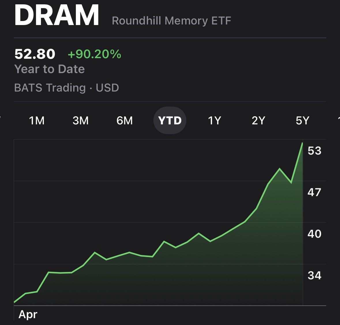
Sometimes I think about putting my entire $30k portfolio into $DRAM, betting on memory becoming a key part in AI, and holding for the next 40 years.
I’m currently 18, would this be a smart idea?

English

What if..... The most obvious big CPO winner was accessible to buy in the US all along? $HIMX
English

I read Goldman Sachs’ AI report, and I was genuinely impressed.
The core insight is as follows:
Agentic AI could turn AI from a capex-heavy cost burden into a business where usage growth drives margin expansion. As token costs fall, more complex agents become economically viable. These agents then consume far more tokens through longer context windows, repeated reasoning loops, validation, tool use, and always-on background monitoring.
This increase in token usage improves infrastructure utilization, strengthens unit economics, and gives hyperscalers and model providers more room to reinvest in model quality, distribution, and capacity.
In other words, the bull case for AI capex is not simply that usage will grow. It is that this usage growth can increasingly flow through at attractive incremental margins. Goldman Sachs argues that this margin inflection is beginning to appear from 2026 onward.

Jukan@jukan05
We have only just entered the early innings.
English
$AXTI - Intel cited rising substrate wafers cost increases
Jukan@jukan05
Intel cited rising substrate, T-glass, and memory costs as headwinds to gross margin in the second half of the year.
English
Samsung Electronics Decides on NAND Expansion Investment at Pyeongtaek P5
Following SK Hynix, Samsung Electronics is also preparing a NAND flash expansion investment. The move reflects rising NAND demand from AI applications, which has driven a significant increase in average selling prices (ASP). The industry estimates that Samsung Electronics' NAND blended margin approached 50% in Q1 this year.
The NAND expansion will take place at Pyeongtaek Campus Plant 5 (P5), which is currently under construction. This marks Samsung's first meaningful NAND expansion since P3. Amid the prolonged industry downturn, Samsung had focused exclusively on DRAM investment at P4.
According to industry sources on the 14th, Samsung Electronics has decided to build a NAND line at Pyeongtaek P5, where cleanroom opening is scheduled for next year. Given the investment timing, a 10th-generation (V10) NAND line is expected to be installed.
This represents Samsung's first large-scale NAND expansion in roughly five years since P3. After NAND market conditions deteriorated from 2022 onward, Samsung concentrated its capex on DRAM equipment rather than building new NAND lines at production bases such as P4, carrying out only limited technology migration (conversion) investment for NAND. The NAND investment planned for this year will likewise be conversion-centric.
The decision to pursue greenfield NAND expansion was driven by rising NAND prices. As AI demand has broadened from training-centric workloads into inference, NAND demand has grown alongside it. On the back of this trend, Samsung Electronics is reported to have generated over 10 trillion won in operating profit from its NAND business alone in Q1 this year. Some forecasts even call for NAND operating margins to exceed 60% in the second half of the year.
P5, currently under construction, is a mega-scale semiconductor production base comprising six phases in total. Cleanroom buildout was originally scheduled for around end-2026, but the timeline has been pulled forward as supply-demand imbalances emerged in both DRAM and NAND. As a result, fab operation is now expected to begin around mid-2028.
Within P5, Samsung has decided to configure a portion of the lines for NAND. However, the specific expansion scale has not yet been finalized, and is expected to be flexibly adjusted based on NAND demand conditions.
A source familiar with Samsung Electronics explained, "P5 will be composed of six phases in total, and the plan under discussion is to build a NAND line in one of these phases," adding, "The investment scale may vary depending on market conditions, but the NAND expansion investment itself is confirmed."
With NAND investment now decided for P5, further NAND investment is expected to follow at P5 Fab 2. Samsung Electronics is preparing to build 'P5 Fab 2' as a twin fab to P5. Sharing the same structure, P5 Fab 2 will also be constructed on a scale of three floors and six phases.
English
Sin retweetledi
DigiTimes published a report on TSMC's packaging this morning, and there's a lot of alpha in it.
To summarize:
1. TSMC is significantly expanding SoIC capacity in 2027 (from 10K wafers/month to 50K wafers/month), with NVIDIA locking up most of this SoIC capacity. Only 10% will be allocated to CPO.
-> Positive for BESI. More hybrid bonding tool orders should follow.
2. CoPoS is delayed… first product shipment expected in Q4 2030.
CoWoS's lifespan is now expected to be longer than previously anticipated. CoPoS is just too difficult to push through. According to DigiTimes, with large orders pouring in not only from NVIDIA and AMD but also from ASIC customers, TSMC's CoWoS capacity for the next two years is already fully booked. CoPoS was originally expected to take the baton with mass production in 2028, but per the latest schedule:
Q3 2026: R&D equipment move-in begins. R&D line buildout takes about 1 year.
Q3 2027: Pilot line equipment orders placed. Equipment lead time of about 3 quarters.
Q2 2028: Pilot tools moved into the Chiayi P7 fab. Validation and fine-tuning needed for about 1 year afterward.
Mid-to-late 2029: Mass production equipment finalized, supply chain orders placed. Lead time of 3 quarters.
Q1 2030: Mass production equipment move-in. First packaging product shipment possible 6 months to 1 year later, in Q4 2030.
In particular, "uniformity" and "warpage" are reportedly causing significant difficulties in implementing CoPoS.
-> Negative for the CoPoS supply chain. TSMC is reportedly even imposing a policy that anyone joining the CoPoS development effort will be barred from selling externally.
3. Lastly, the CoWoP project led by NVIDIA and SPIL (矽品) is reportedly facing a potential suspension. Because of the higher technical difficulty and elevated cost, SPIL and Taiwanese PCB vendors are showing low willingness to participate, and only Chinese PCB vendors are showing intent to continue R&D.
-> Those who were pushing CoWoP should be ashamed of themselves. The ones who were pumping mainland Chinese names...
English
$AXTI Jensen is bullish on photonics!! Will we see $100?
Sin@sinuwy
photonics stocks dumping this morning, as you know Jensen is adamant on copper…. But math does not lie…. $AXTI
English

$ETH to $3k is imminent…. narrative needs to change
Watcher.Guru@WatcherGuru
JUST IN: ETH reclaims $2,350, rising over 8% today.
English
