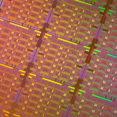
Tom Wassick

1.4K posts

Tom Wassick

Tom Wassick

@wassickt

Semiconductor packaging engineering professional working on upcoming server technology while also watching chip and packaging technologies. Opinions are mine.

Lagrangeville, NY Katılım Ekim 2010
221 Takip Edilen959 Takipçiler
High Yield
High Yield@highyieldYT·
What's the best way to automate a teardown/die shot process? Especially the manual lapping part? I'm thinking a gemstone lapping machine with 30 to 3 micron lapping film and maybe something that can produce even pressure on the entire die.
English
3
0
6
995
Tom Wassick
Tom Wassick@wassickt·
@jukan05 So, the building block is a 2 die with 4 hbm, most likely in a CoWoS-L config. They then take 2 of those and either use the laminate to integrate them, or have a 2nd CoWoS (L?) to stitch them together for the 2+2?
English
1
0
5
937
Jukan
Jukan@jukan05·
[GF Securities Overseas Electronics & Communications] Regarding Rubin Ultra being designed as a 2-die configuration (versus the market expectation of 4-die): We believe TSMC’s output is 2-die, and there are currently two versions — Rubin Ultra 2-die and Rubin Ultra 2+2 dies. The 2+2 scheme involves TSMC producing 2-die units, which are then assembled into a 2+2 die configuration on a PCB/CoWoS board. Subsequently, a single Kyber compute blade would consist of either four 2-die units or two 2+2 die units. Therefore, the overall impact on value is very limited (our view is also consistent with the roadmap shown at GTC). On the memory side, high-capacity HBM4E (64GB per cube) is used — Rubin Ultra 2-die carries 512GB (8 × 64GB), and when assembled into the 2+2 die configuration, it reaches 1,024GB (in line with original expectations). Conversely, we believe the areas where value could be negatively impacted are packaging, testing, etc. As for rack quantities, there is no impact.​​​​​​​​​​​​​​​​ $NVDA
Jukan@jukan05

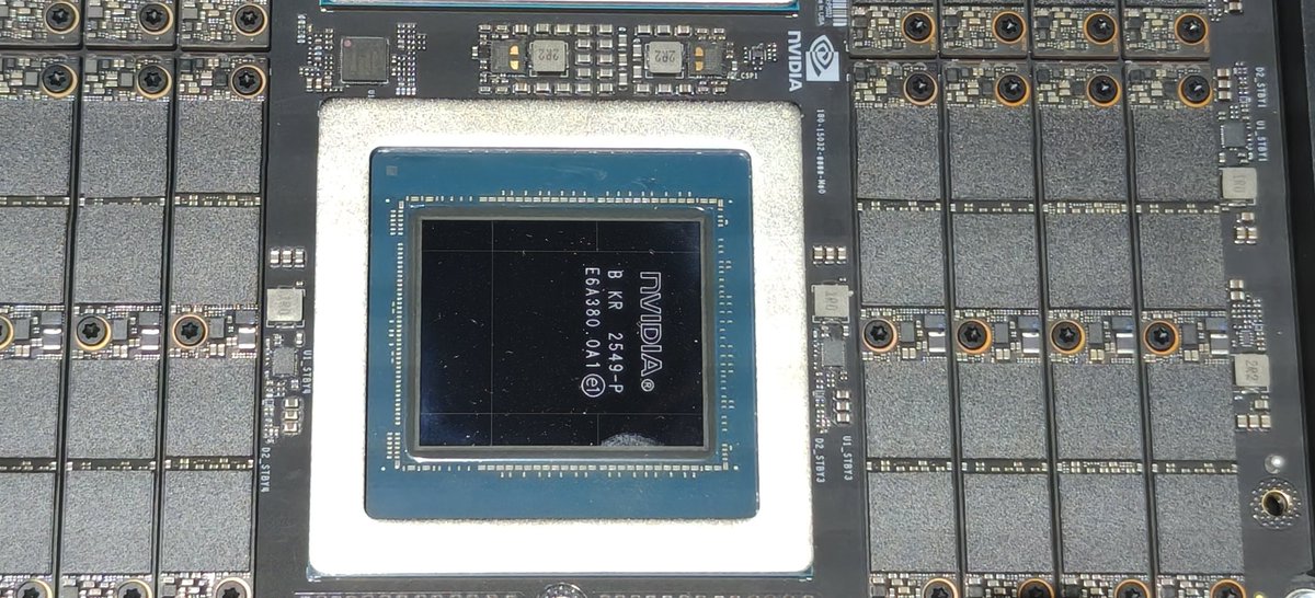
Rumor: The 4-die Rubin Ultra has been canceled, and only the 2-die Rubin Ultra will be mass-produced. It is still unclear whether this will result in a reduction in Rubin Ultra’s HBM capacity.

English
6
17
137
78.1K
Tom Wassick
Tom Wassick@wassickt·
@Silicon_Fly @JustMyT01 Oh so wrong, perception is more important than you may realize, and people will look at that and dismiss you if they aren’t familiar with your stuff
English
1
1
2
45
JustMyThoughts
JustMyThoughts@JustMyT01·
Low level thinkers like you lack the imagination to create. Allow does who can create. Stop Bitching. It's screaming attention seeking
English
0
0
0
698
Vengineerの妄想
Vengineerの妄想@Vengineer·
Samsung HBM4のパッケージの裏 赤で囲った部分がI/Oですかね。 そうなると、1024ビットが2組って感じですかね。
Vengineerの妄想 tweet media
日本語
1
0
8
569
Tom Wassick
Tom Wassick@wassickt·
@dnystedt Am waiting to see when it gets “down to” the advanced packaging talent search…
English
1
0
2
2.2K
Dan Nystedt
Dan Nystedt@dnystedt·
Tesla’s TeraFab has launched a talent war in Taiwan via job postings seeking senior chip experts (Process Integration Engineers) with over 10-years of experience, media report, adding its 2nm fab plan aims directly at TSMC. Chip engineers are already in short supply in Taiwan – like nearly everything chip related – and industry insiders worry the ‘Musk Halo Effect’ will draw local talent. More: Deep expertise in FinFET, GAA, BSPDN, and across all stages of chip building: FEOL, MOL and BEOL. $TSLA $TSM $UMC $ASX #semiconductors #semiconductor money.udn.com/money/story/56…
English
58
162
1.8K
610.6K
Tom Wassick
Tom Wassick@wassickt·
@jukan05 One comment, dicing lasers have already transitioned from nano to pico, femto is just the next jump
English
0
0
0
143
Jukan
Jukan@jukan05·
Samsung Electronics to Enhance HBM4 Quality with Next-Generation Wafer Dicing Process Samsung Electronics is transitioning its wafer dicing process — a critical step directly tied to semiconductor quality and yield — to a next-generation approach. The company plans to expand its application of "femtosecond (one-quadrillionth of a second) laser" technology, which was first introduced last year targeting High Bandwidth Memory (HBM4), in a move to assert dominance in the HBM4 market through dramatically improved cutting precision. According to industry sources on the 23rd, Samsung Electronics is placing orders for wafer dicing equipment equipped with femtosecond laser technology. The equipment covers both "grooving" — which scores the wafer surface — and "full-cut" tools, with the initial procurement volume standing at a minimum of 10 units. The equipment is slated for installation at Samsung's Cheonan campus, where advanced semiconductor packaging operations are conducted, and purchase orders (POs) are currently being prepared. Samsung is also reviewing the option of placing additional orders to secure as large a volume as possible. Given that lead times for wafer dicing equipment exceed eight months, the intent is to secure supply proactively while substantially expanding the scope of femtosecond laser-based dicing processes. A well-placed industry source noted, "Even after the initial introduction, Samsung Electronics is in ongoing discussions with partners to continue scaling up femtosecond grooving and full-cut equipment," adding that it represents "an attempt to convert the majority of wafer dicing processes to the next-generation approach." In semiconductor manufacturing, a dicing process — which separates wafers into individual chip units (dies) — is essential following the front-end process where circuits are etched onto wafers. Conventional dicing has largely relied on mechanical cutting via diamond wheel blades. While lasers have been used in some cases, the laser pulse duration — the key measure of precision — has remained at the nanosecond (one-billionth of a second) level. Femtosecond lasers generate pulses at the one-quadrillionth-of-a-second scale, enabling far finer cuts compared to both conventional mechanical methods and nanosecond lasers. The technology can cut without affecting the ultra-fine circuitry and interconnects of advanced semiconductors, while also minimizing particle contamination generated during the dicing process — ultimately maximizing the quality of the finished semiconductor. Samsung Electronics first introduced femtosecond laser dicing in Q2 of last year. At the time, only a handful of units were deployed, but having demonstrated improvements in performance and productivity, the company has decided to scale up adoption. Samsung plans to apply femtosecond laser dicing to HBM4 processes as a priority, with the goal of improving HBM4 yield and productivity. Samsung recently commenced mass production shipments of HBM4. Demand for femtosecond laser dicing is expected to grow in tandem with the ramp-up schedule for full-scale mass production. The company is also reportedly evaluating the introduction of femtosecond laser dicing for products beyond DRAM, including NAND flash and system semiconductors. Samsung's femtosecond laser dicing supply chain is expected to be handled by domestic firm EO Technics and Japan's Disco. An industry source commented, "Competition between EO Technics and Disco for femtosecond laser dicing orders is set to intensify," adding that "demand for femtosecond laser dicing is rising not only at Samsung Electronics but also at other domestic and international semiconductor manufacturers."
Jukan tweet media
English
6
6
139
58.3K
Tom Wassick
Tom Wassick@wassickt·
Procured Panther Lake, pretty cool that you can clearly see some of the X and Y wiring patterns of the Intel CPU chiplet on the signal side of the BSPDN structure by looking through the die back with an infrared scope. Usually it’s just device patterns and crack stops visible
English
0
0
6
263
Tom Wassick
Tom Wassick@wassickt·
@NuttyCLD A bit pessimistic on the organic wiring density there, though it depends on your specific metric, which isn’t clearly stated. Line widths on organic are sub 10um, RFP pitches are in the hundreds. When I hear wiring, I think line widths and spaces
English
1
0
2
139
Nutty
Nutty@NuttyCLD·
This table clearly highlights the strengths and weaknesses of organic, silicon, and glass materials when used as interposers or substrates.
Nutty tweet media
Nutty@NuttyCLD

x.com/i/article/2021…

English
2
12
93
19.5K
Tom Wassick
Tom Wassick@wassickt·
@jukan05 That 20c number is very, very pessimistic. Thermal models I’ve seen indicate that it’s more like 3-5, and that’s without mitigation schemes. A few degrees is manageable
English
0
2
14
1.2K
Jukan
Jukan@jukan05·
Why It’s Extremely Difficult to Manufacture Mobile SoCs on Intel 18A/14A (Perspective from an Active Design House Industry Professional, via SemiWiki) – #1
Jukan tweet media
English
16
13
168
69.7K
Tom Wassick
Tom Wassick@wassickt·
@IanCutress @Microsoft @Azure Ask them for a real picture -- that one doesn't make technical sense -- and was likely computer "enhanced" One of their videos shows it's more like this:
Tom Wassick tweet media
English
0
1
10
4.7K
Andreas Schilling 🇺🇦
Andreas Schilling 🇺🇦@aschilling·
Microsoft Maia 200 is deployed for @Azure - 3 nm TSMC - 140 billion transistors - 750 W TDP - 216 GB HBM3e at 7 TB/s - 272 MB SRAM - 10 PFLOPS FP4 - 5 PLOPS FP8
Andreas Schilling 🇺🇦 tweet mediaAndreas Schilling 🇺🇦 tweet mediaAndreas Schilling 🇺🇦 tweet mediaAndreas Schilling 🇺🇦 tweet media
Indonesia
11
64
455
28.2K
Tom Wassick
Tom Wassick@wassickt·
@aschilling @Azure I’m not sure I truly believe either of the images, as the HBM aspect ratio seems off on the other flavor. Suspect reality is somewhere in between
English
1
0
0
187
Chris S. Cornell
Chris S. Cornell@BiggestComeback·
@JeffryGerberMD They have been shoveling… cars won’t be needed until tomorrow at the earliest. Thanks!
English
2
0
2
115
Chris S. Cornell
Chris S. Cornell@BiggestComeback·
Predictably, my flight home to NY was cancelled this morning… Headed home from Florida on Wednesday. Meanwhile, here’s a view of my driveway back home…
Chris S. Cornell tweet media
English
9
0
44
2.2K
Tom Wassick
Tom Wassick@wassickt·
@zephyr_z9 The substrate core changes to glass, they’ll still use abf in the wiring layers
English
0
0
2
572
Zephyr
Zephyr@zephyr_z9·
I think they are talking about replacing ABF with glass in the IC substrate
Jukan@jukan05

@rwang07 What the hell is Glass substrate DRAM?

English
4
1
43
34K