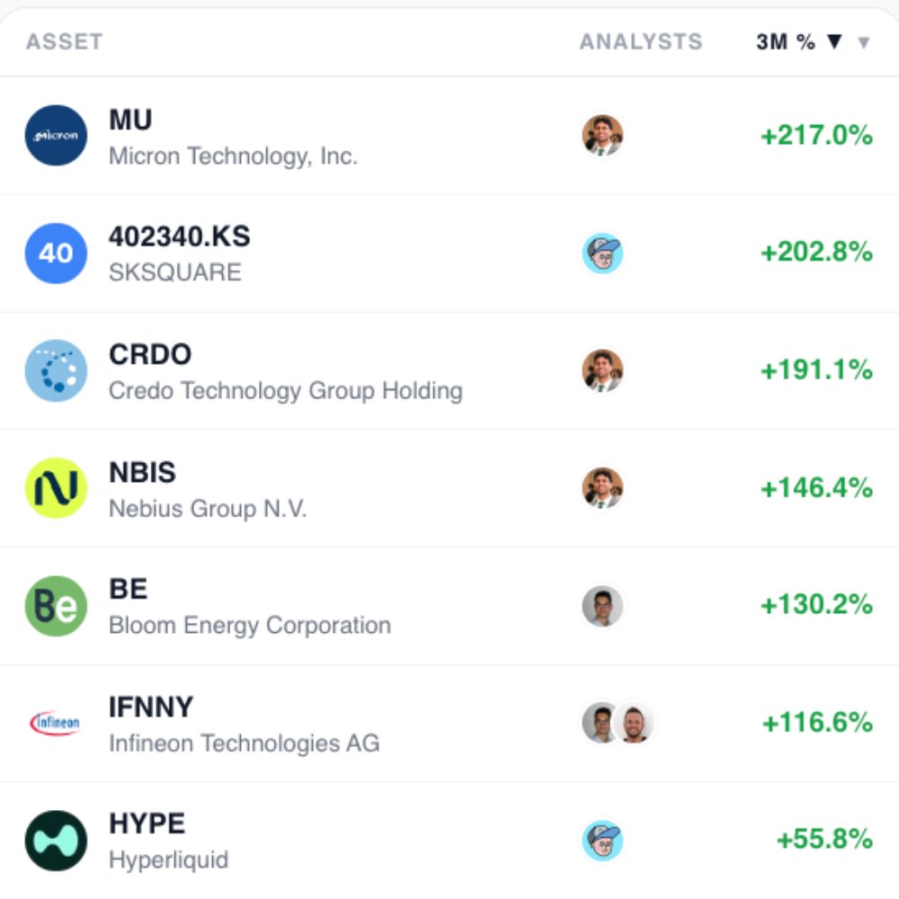
Закреплённый твит

Total wafer fab equipment spending is projected to reach $145 billion in 2026, $200 billion in 2027 and $250 billion in 2028, a near doubling in three years driven almost entirely by HBM and advanced logic demand (Save this).
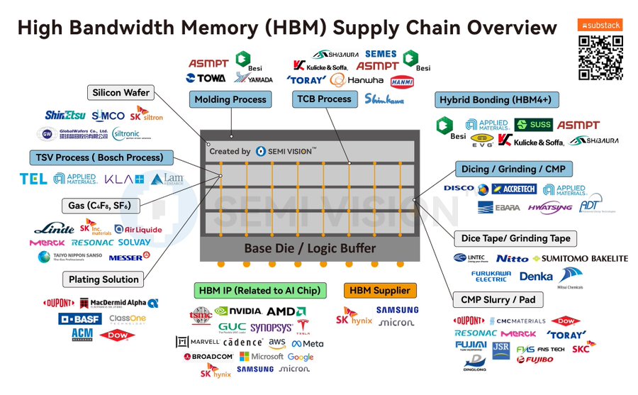
And this image above shows exactly who collects a toll on every single chip that gets built.
Before any HBM chip can exist, you need an ultra pure silicon wafer to build it on.
Shin-Etsu Chemical and Siltronic are the dominant global silicon wafer suppliers, with Shin-Etsu controlling roughly 30% of global supply, one of the quietest monopolies in all of semiconductors.
The most technically complex step is the TSV process drilling microscopic vertical holes through each silicon die so electrical signals can travel between stacked layers.
Tokyo Electron (TEL), Applied Materials (AMAT), KLA Corporation (KLAC), and Lam Research (LRCX) dominate this step,and all four beat earnings, raised guidance, and reported sold out capacity simultaneously in the most recent cycle, an extraordinarily rare alignment that signals just how tight the HBM supply chain truly is.
Applied Materials leads in deposition tools, Lam Research controls roughly 50% of the global etch market, and KLA holds a near monopoly at 55% share in process control and inspection, every wafer must pass through KLA's equipment to confirm chip integrity before moving forward.
The TSV etching process also requires specialized industrial gases, C4F8 and SF6 that create the precise chemical reactions needed to carve through silicon without damaging surrounding material.
Linde, Air Liquide, SK Materials, and Merck supply these gases and none of them are substitutable within current production timelines making them some of the most overlooked AI infrastructure plays in the market.
Once the dies are prepared, they need to be stacked and bonded together, currently via Thermal Compression Bonding, but the industry is shifting toward Hybrid Bonding for HBM4 and beyond.
Besi, ASMPT, Hanmi Semiconductor, and Kulicke & Soffa dominate the bonding equipment market, and the hybrid bonder market alone is projected to reach nearly $2 billion by 2028 as every memory maker upgrades to the next-generation process.
After stacking, chips need to be thinned, cut and polished through grinding, dicing, and CMP processes where DISCO Corporation holds near-monopoly control in precision dicing equipment, with DuPont, Dow, CMC Materials, and Resonac supplying the CMP slurry chemicals needed to polish chips to atomic smoothness.
All of this feeds into just three companies that actually build and sell HBM, SK Hynix with over 50% global market share, Micron ramping HBM4 for Nvidia's Rubin platform and Samsung fighting to regain ground after falling behind on qualification timelines.
And at the very bottom of the supply chain sits the demand engine, every hyperscaler and chip designer whose AI accelerators require HBM to function, Nvidia, AMD, Broadcom, Google, Microsoft, Meta, AWS, Marvell, and Tesla.
Every company in this supply chain is a toll booth and the traffic is only getting heavier.
Make sure to follow me @MelvinInvests for more semiconductor opportunities.
English