RayPCB

10.8K posts

RayPCB banner
RayPCB

RayPCB

@RaymingTech

RAYPCB | Since 2005 🌍 🔌 Premium PCB Manufacturing ⚡ Reliable PCB Assembly (PCBA) 💡 Contract EMS Supplier ✨ Fast Turnkey Solutions | Global Shipping

shenzhen เข้าร่วม Ocak 2017
4.2K กำลังติดตาม2.5K ผู้ติดตาม
RayPCB
RayPCB@RaymingTech·
Designed & Simulated a 50-Ω Microstrip Transmission Line for 5GHz Operation ⚡ In RF engineering, a poorly matched impedance doesn't just degrade performance — it reflects energy back into your source and kills your design. So I put theory to practice. Using an FR4 substrate as my foundation, I modeled a microstrip trace geometry optimized for maximum power transfer and minimal signal distortion at 5GHz. 📐 Design Parameters Substrate: FR4 | εᵣ = 4.4 | h = 1.6mm Trace Width: 3mm | Trace Length: 8mm Electrical Length: 90° (Quarter-wavelength) at 5GHz 📊 What the Simulation Revealed ✅ Return Loss (S11) of -35 dB — near-zero reflection, essentially all power delivered to the load ✅ Precise phase control — 8mm physical length dialed in to hit an exact 90° electrical length ✅ E-field visualization confirmed smooth wave propagation and clean electromagnetic energy confinement within the dielectric The most valuable takeaway? Physical dimensions are not arbitrary — every millimeter shapes how electromagnetic energy travels, bends, and behaves. Next step: scaling these principles into multi-element feeding networks and antenna arrays. If you're working in RF, microwave design, or antenna engineering — let's connect. 🚀 #FEngineering #MicrowaveEngineering #AntennaDesign #EMSimulation #5G #SignalIntegrity #EEDesign
English
0
0
2
36
RayPCB
RayPCB@RaymingTech·
5 Common High-Speed PCB Length Matching Mistakes (That 90% of Engineers Make) Length matching goes far beyond simply making trace lengths equal — it’s a critical factor in preserving signal integrity. Here are some frequent pitfalls to watch out for: 1️⃣ Overlooking the return path Equal trace length doesn’t guarantee equal delay if the reference plane is disrupted. 2️⃣ Excessive serpentine routing Too-tight serpentine patterns increase crosstalk and cause delay distortion. 3️⃣ Neglecting differential pair skew The timing difference between pair lines impacts performance more than absolute length. 4️⃣ Over-applying length matching Not every signal demands strict length control—know when it’s necessary. 5️⃣ Ignoring manufacturing tolerances Real-world boards often differ from simulation results due to fabrication variations. Key takeaway: Length matching is a means to an end, not the end itself. The real goal is ensuring robust signal integrity. What’s the toughest challenge you face when designing high-speed PCBs? Let’s discuss!
RayPCB tweet media
English
0
0
22
763
RayPCB
RayPCB@RaymingTech·
SMT First Article Test
English
0
0
1
171
RayPCB
RayPCB@RaymingTech·
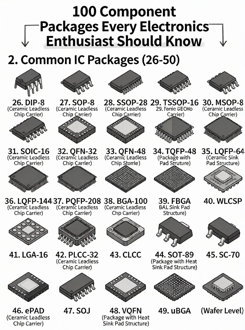
🔧 The package matters just as much as the component itself. In electronics design and embedded systems, selecting the right IC package can make or break your product — affecting everything from thermal performance and signal integrity to board space and manufacturability. Whether you're routing a PCB, troubleshooting a hardware issue, or scaling toward production, knowing your packages is a fundamental skill. 📦 From through-hole to advanced surface-mount: DIP — reliable, breadboard-friendly, easy to prototype SOP/SOIC — compact, widely supported in SMT lines QFN — excellent thermal dissipation, minimal footprint BGA — high pin density for complex, high-performance ICs This reference covers 26–50 commonly used IC packages, giving engineers and hardware enthusiasts a practical visual guide to recognizing and differentiating them in real-world designs. 💡 If you're growing in electronics, PCB design, or embedded systems — bookmark this. You'll reference it more than you think. ♻️ Repost if you find this useful — let's help the engineering community level up together. #Electronics #EmbeddedSystems #PCBDesign #HardwareEngineering #EE #CircuitDesign #Engineering
RayPCB tweet media
English
0
17
92
2.8K
RayPCB
RayPCB@RaymingTech·
Capacitors in Real-Life Circuits ⚡ Continuing my 21-Day Electronics Learning Challenge – today’s focus: how capacitors are actually used in practical applications, beyond textbook theory. Where capacitors shine in real circuits: 🔹 Power Supply Filtering – smooths voltage and reduces noise 🔹 Coupling – passes AC signals while blocking DC 🔹 Decoupling – stabilizes voltage, especially for ICs 🔹 Timing Circuits – enables delays and oscillators Real-world examples you’ve likely used: 📱 Mobile chargers → stable DC output 🎧 Audio systems → cleaner sound with less noise 🖥️ Microcontrollers → reliable operation thanks to decoupling capacitors Key insight: Capacitors may be small, but they’re essential for building circuits that are reliable, efficient, and noise-free. Moving from storing charge to improving performance – understanding how components work in real applications makes all the difference.
RayPCB tweet media
English
2
28
190
4.2K
RayPCB
RayPCB@RaymingTech·
SMT Component Selective Protection - Perimeter Dam Rubber Filling Process
English
0
0
0
177
RayPCB
RayPCB@RaymingTech·
Replacing damaged components
English
0
2
18
1.4K
RayPCB
RayPCB@RaymingTech·
🔍 Microcontroller vs. Microprocessor: Not the same thing. These terms are often used interchangeably, but they serve very different roles in electronics and embedded systems. 🧠 Microcontroller (MCU) An all-in-one chip designed for dedicated control tasks. Includes: ✔ CPU ✔ Memory ✔ I/O peripherals ✔ Timers & communication interfaces ✅ Best for: → Embedded systems → IoT devices → Home appliances → Industrial controllers 💻 Microprocessor (MPU) A CPU-only chip that relies on external memory and peripherals to function. ✅ Best for: → Computers & laptops → Complex operating systems → High-performance applications → Advanced processing tasks 📌 Why it matters Engineers, designers, and sourcing pros: choosing between an MCU and MPU impacts cost, power efficiency, and performance. The right decision early on saves major time and money later. Which component comparison should I cover next? #EmbeddedSystems #ElectronicsEngineering #Microcontroller #Microprocessor #ProductDesign #HardwareDesign
RayPCB tweet media
English
0
10
59
1.5K
RayPCB
RayPCB@RaymingTech·
PCBA - Through the wave soldering process
English
1
1
19
1.4K
RayPCB
RayPCB@RaymingTech·
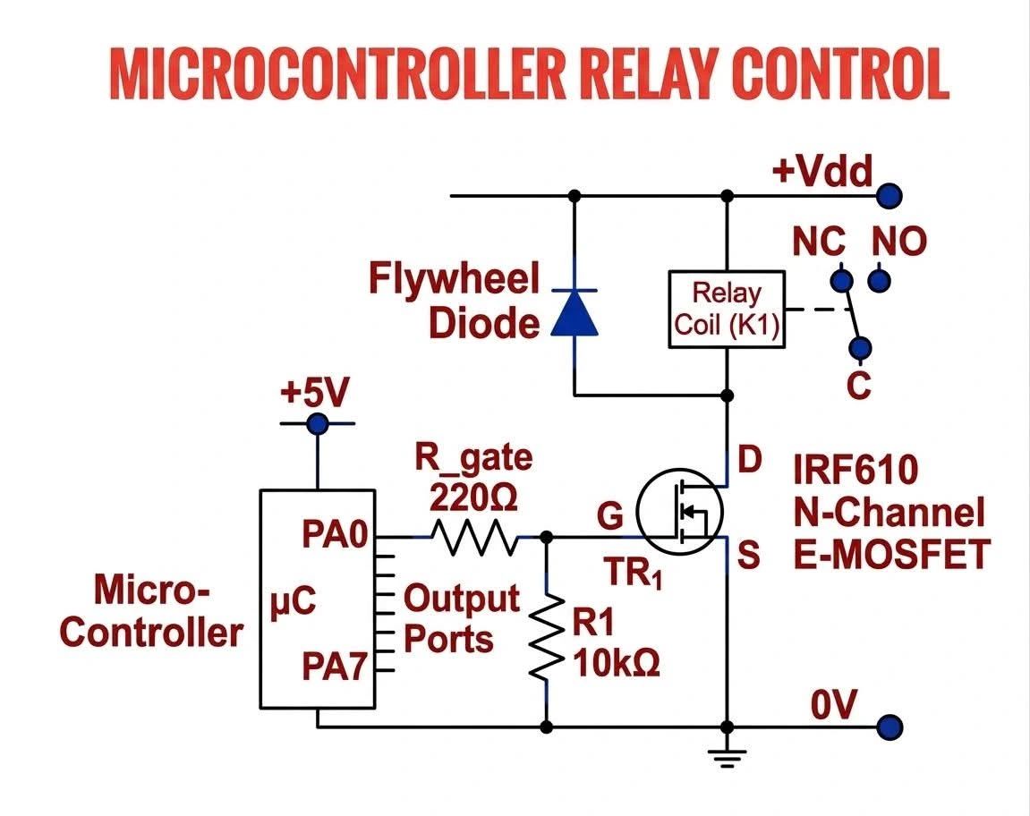
Ever wondered how a microcontroller switches a high-power load without getting fried? Here's a simple but powerful circuit that does exactly that — using a MOSFET as the bridge between logic and load. Here's how it works: When the microcontroller's output pin (PA0) goes HIGH, it triggers the MOSFET gate through a 220Ω resistor. The MOSFET switches ON, completing the path to ground and energizing the relay coil — flipping the contact from NC to NO. When PA0 goes LOW, the MOSFET cuts off, the coil de-energizes, and the relay snaps back to its default NC state. Two small components do a lot of the heavy lifting here: → A 10kΩ pull-down resistor keeps the MOSFET firmly OFF when no signal is present — no floating pins, no false triggers. → A flywheel diode clamps the voltage spike generated when the relay coil collapses — protecting the MOSFET from a potentially damaging kickback. It's a compact, reliable design that's become a staple in embedded systems — anywhere you need low-power logic to command a high-power world. Simple concept. Endless applications. #EmbeddedSystems #Electronics #CircuitDesign #Engineering #Microcontrollers #HardwareEngineering
RayPCB tweet media
English
2
11
52
1.3K
RayPCB
RayPCB@RaymingTech·
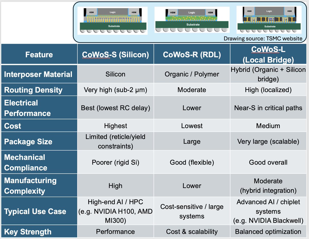
GPUs used to sit on PCBs next to GDDR memory, talking to each other through long board traces. That worked — until it didn't. Long interconnects meant high RC delay, limited I/O density, lower bandwidth, and more energy burned per bit. As AI workloads scaled, the architecture hit a wall. The industry's answer: heterogeneous integration — pulling logic and memory into a single package. TSMC's Chip-on-Wafer-on-Substrate (CoWoS) is one of the most important enablers of this shift. The idea is straightforward: place the GPU and HBM side-by-side, connect them through a fine-pitch interposer, and eliminate the long PCB traces that were killing performance. The interposer is the key piece here. It's a high-density wiring layer that enables short die-to-die connections, fine-pitch routing, and bridges chip I/O to the package. Two main flavors exist — silicon (precise, expensive) and organic RDL (cheaper, larger area). CoWoS comes in three variants, each making a different tradeoff: CoWoS-S uses a silicon interposer with ~0.5–2 µm routing. Maximum density and performance, but limited by reticle size and cost. CoWoS-R uses an organic RDL substrate. Lower cost, larger footprint, more flexibility — with some density tradeoff. CoWoS-L combines an organic base with localized silicon bridges only where high density matters most (think: GPU-to-HBM interface). It's the architecture showing up in large-scale AI systems because it balances performance, cost, and scalability. The bottom line: CoWoS replaces long PCB interconnects with fine-pitch packaging — and that shift is a big part of why modern AI accelerators can deliver the bandwidth they do. (Comparison table in the comments.) #Semiconductors #AdvancedPackaging #CoWoS #HeterogeneousIntegration #Chiplets #AIHardware #HPC #TSMC #HBM #ElectronicsEngineering
RayPCB tweet media
English
0
0
5
366
RayPCB
RayPCB@RaymingTech·
5 EMI Mistakes Engineers Overlook—Until It’s Too Late You’ve nailed the PCB design review, but then the EMC test fails. Sound familiar? You’re not alone. In fact, over 70% of EMI headaches stem from just a handful of preventable mistakes—yet these slip through in real-world projects far too often. Here are the top 5 EMI pitfalls that can derail your design—and how to avoid them: ❌ 1. Neglecting Return Path Design Signals don’t just go forward—they return. Interrupting that return path with splits, gaps, or poor layer transitions turns your PCB into an antenna. Quick fixes: 🔹 Maintain continuous reference planes 🔹 Avoid crossing split planes 🔹 Place stitching vias near transitions ❌ 2. Overlooking Ground Integrity “All grounds are created equal” is a myth that kills signal integrity. Fragmented or noisy grounds cause unstable references—fueling EMI. Quick fixes: 🔹 Use solid ground planes 🔹 Keep ground impedance low 🔹 Separate noisy and sensitive zones ❌ 3. Messy Power Distribution Network (PDN) Your power plane is a hidden culprit. Inadequate decoupling leads to voltage ripple—and unwanted emissions. Quick fixes: 🔹 Put decoupling capacitors close to IC pins 🔹 Use a mix of capacitor values 🔹 Optimize PDN impedance ❌ 4. Poor High-Speed Routing Sharp corners, long stubs, and uncontrolled impedance convert traces into unintended antennas. Quick fixes: 🔹 Control impedance carefully 🔹 Avoid stubs 🔹 Route with smooth, continuous paths ❌ 5. Waiting Too Long to Shield & Filter Trying to patch EMI issues post-layout? That’s like trying to patch a leaking pipe with tape. Quick fixes: 🔹 Add filters early—common-mode chokes, ferrites 🔹 Apply shielding where needed 🔹 Consider EMI from day one A Final Thought EMI problems aren’t born from complex issues—they’re born from small design slip-ups repeated across the board. Nail the fundamentals, and you can eliminate 80% of EMI risks. 🔁 Your Turn: What EMI challenge has been your toughest to tackle? Share your stories and solutions below!
RayPCB tweet media
English
1
5
29
1.2K
RayPCB
RayPCB@RaymingTech·
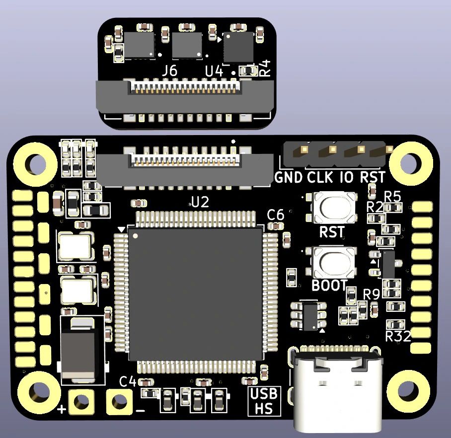
Excited to share the hardware design of a high-performance UAV flight controller inspired by the Cube Orange platform. Centered around the powerful STM32H7 microcontroller, this system’s complete schematic and PCB were expertly crafted using the open-source KiCad software. Key hardware highlights include: • Triple redundant IMUs and dual barometers to ensure robust state estimation and fault tolerance • Dual CAN-FD interfaces to support high-speed communication with UAV peripherals • Multiple UART ports dedicated to GPS, telemetry, and RC connectivity • High-rate flight data logging enabled by microSD storage via SDMMC • External SPI flash memory for firmware and parameter storage • USB-C device interface to facilitate firmware updates and MAVLink communication • Direct 6S LiPo battery input (up to 25.2 V) paired with a 5 V buck regulator and isolated 3.3 V rails for digital logic and sensitive sensors The design leverages a 6-layer PCB structure featuring controlled grounding, distinct power domains, and strategic sensor isolation. To minimize vibration and electrical noise interference, IMUs are mounted on a dedicated sensor section connected via a flex cable, effectively isolating them from power and digital noise sources. This careful attention to hardware architecture aims to maximize reliability and performance for demanding UAV applications.
RayPCB tweet mediaRayPCB tweet mediaRayPCB tweet mediaRayPCB tweet media
English
0
0
5
231
RayPCB
RayPCB@RaymingTech·
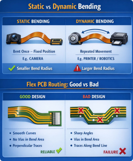
Master Flex PCB Bending Radius in Just 60 Seconds Flexible PCBs are revolutionizing electronics — making devices smaller, lighter, and more reliable than ever. But one critical detail often overlooked by engineers? The bending radius. Why does it matter? Bending too sharply risks: • Cracked copper layers • Delamination of materials • Premature circuit failure Here’s a quick guide: Minimum bend radius depends on your PCB thickness: • Single-layer flex: ≥ 6 × thickness • Double-layer flex: ≥ 12 × thickness • Multilayer flex: ≥ 20 × thickness For example, a 0.10 mm thick flex PCB requires: • Single-layer → 0.6 mm bend radius • Double-layer → 1.2 mm bend radius Static vs Dynamic Bending — Know the Difference Static bending: Bent once during assembly and fixed. Common in camera modules, consumer electronics, medical devices. → Smaller bend radius is acceptable. Dynamic bending: Repeated motion during use. Found in printers, robotics, automotive systems. → Aim for ≥ 20–40 × thickness to avoid failures. Pro Tips Most Engineers Miss: ✔ Avoid placing vias at bend areas ✔ Route traces perpendicular to bending direction ✔ Use rolled annealed copper (RA) for flexibility ✔ Steer clear of sharp angles ✔ Keep components well away from bend zones Getting your bend radius right from the start saves headaches, costly redesigns, and improves product durability. We’ve supported countless projects with extensive flex and rigid-flex designs — providing deep engineering and DFM expertise. If you want a quick, no-obligation design check, just reach out. Let’s make your flex PCB design bulletproof!
RayPCB tweet media
English
1
2
17
898
RayPCB
RayPCB@RaymingTech·
PCB SMT Tooling Function Test
English
0
1
8
555
RayPCB
RayPCB@RaymingTech·
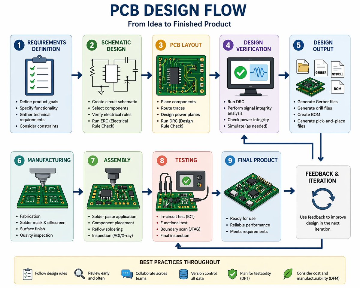
✓ The Complete PCB Design Flow – From Concept to Finished Product Many assume PCB design is just about routing traces — but in reality, it’s a detailed engineering journey involving multiple critical stages. Let’s walk through the process step-by-step: 1️⃣ Requirements – Define the product’s purpose and goals. 2️⃣ Schematic Design – Translate your idea into an electronic circuit diagram. 3️⃣ PCB Layout – Strategically place components and route all connections. 4️⃣ Verification – Perform thorough checks for design rule compliance and signal integrity. 5️⃣ Output Generation – Create Gerber files and Bill of Materials (BOM) for manufacturing. 6️⃣ Manufacturing – Fabricate the PCB according to specifications. 7️⃣ Assembly – Mount and solder components onto the board. 8️⃣ Testing – Validate electrical performance and functionality. 9️⃣ Final Product – Deliver a fully functional PCB ready for use. 🔁 Continuous Improvement – Iterate with feedback to enhance performance and reliability. 💡 In essence, successful PCB design is a cyclical process: Idea → Design → Build → Test → Improve. I’d love to hear from you: ✨ Which step do you find most challenging? Share your experience in the comments! 📌 Save this guide for your next PCB project.
RayPCB tweet media
English
1
12
61
2K
RayPCB
RayPCB@RaymingTech·
🚀 Essential IC Types Every Electronics Engineer Should Know From smart home devices to industrial automation—Integrated Circuits (ICs) are the unsung heroes behind modern electronics. If you're designing or troubleshooting electronic systems, knowing these IC categories is non-negotiable. Here’s a practical breakdown: 🧠 Brain & Control → Microprocessor (CPU): Computing powerhouse (e.g., Intel Core series) → Microcontroller (MCU): All-in-one control for embedded systems 📶 Signal Processing & Amplification → Op-Amp: High-gain signal amplification → Comparator: Voltage level detection → 555 Timer: Timing, pulse generation, oscillation 🔄 Data Conversion → ADC: Real-world signals → digital data → DAC: Digital → analog signals ⚡ Power & Drive → Voltage Regulator: Stable power supply → Motor Driver IC: Speed & direction control for motors 💾 Memory & Logic → Memory IC (RAM/ROM/EEPROM): Data storage & retrieval → Logic Gates: Digital circuit building blocks 📡 Interface & Sensing → Sensor Interface IC: Bridges sensors to processors for accurate data acquisition Understanding these ICs isn't just academic—it’s the foundation for building smarter, more reliable electronics. Which IC type do you work with most often? 👇
RayPCB tweet media
English
1
18
103
2.6K
RayPCB
RayPCB@RaymingTech·
Heavy Copper PCB
RayPCB tweet media
Dansk
0
0
2
135
RayPCB
RayPCB@RaymingTech·
Driving a heavy load with a single transistor? You might need more base current than expected. Enter the Darlington pair — a simple but powerful configuration that multiplies current gain by cascading transistors. 🔹 Single transistor: Moderate gain (~200) 🔹 Two-transistor Darlington: First transistor’s emitter drives the second’s base → gain up to ~50,000. Trade-off? Higher V_BE (1.2–1.4 V). 🔹 Three-transistor Darlington: Gain beyond 50,000 — control large loads with tiny input current. Downsides: slower switching, higher voltage drop. Key takeaway: Great for low-current control of big loads, but watch out for speed and saturation voltage trade-offs. Have you used a Darlington pair in a design? Or do you prefer MOSFETs for similar applications? 👇 #Electronics #EmbeddedSystems #CircuitDesign #DarlingtonPair #EngineeringTips
RayPCB tweet media
English
1
8
63
1.3K
RayPCB
RayPCB@RaymingTech·
PCB SMT Tooling Function Test #RayPCB
English
0
0
2
247