
RayPCB
10.9K posts


RayPCB
@RaymingTech
RAYPCB | Since 2005 🌍 🔌 Premium PCB Manufacturing ⚡ Reliable PCB Assembly (PCBA) 💡 Contract EMS Supplier ✨ Fast Turnkey Solutions | Global Shipping
shenzhen Joined Ocak 2017
4.2K Following2.5K Followers
Did you know the NAND gate is dubbed the "universal gate" in digital electronics? That’s because you can construct any digital logic circuit using only NAND gates.
Here’s why it’s so powerful:
The NAND gate outputs LOW only when both inputs are HIGH; otherwise, it outputs HIGH.
From this simple behavior, you can build every fundamental logic gate:
NOT gate (Inverter): Tie both inputs together — the output flips the input signal, acting as a NOT gate.
AND gate: NAND gives you an inverted AND. Feeding that output through another NAND (configured as a NOT) yields the standard AND function.
OR gate: Using De Morgan’s law, invert both inputs with NAND-based NOT gates, then feed them to another NAND to create OR.
NOR gate: Create an OR gate as above, then invert its output with a NAND to get NOR.
Buffer: Two NAND inverters in series restore the original input signal.
XOR gate: Combine multiple NANDs cleverly so the output is HIGH only when inputs differ.
XNOR gate: Modify the XOR NAND setup to output HIGH when inputs are the same.
The core insight: NAND gates alone suffice to implement any Boolean function.
This universality simplifies digital design hugely. Engineers can standardize on NAND gates for an entire circuit, streamlining manufacturing and cutting costs — a brilliant example of elegance meeting efficiency in engineering.

English
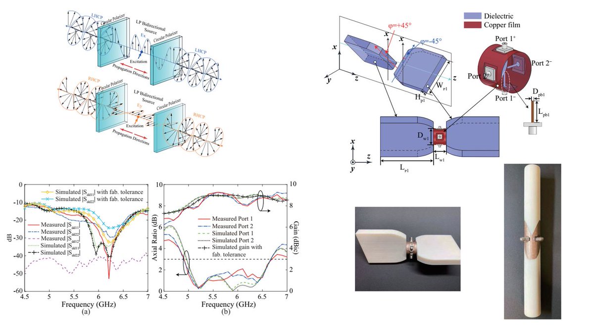
🔁 Understanding Circular Polarization (CP) Sense in Antenna Design
I recently came across a fascinating paper on additively manufactured bidirectional circularly polarized antennas. One concept that really stood out: CP sense.
👉 In simple terms, CP sense describes the rotation direction of the electric field as the wave travels:
RHCP → clockwise rotation
LHCP → counterclockwise rotation
What makes this research unique? The antenna achieves same-sense radiation in opposite directions.
📡 Traditionally: opposite directions → opposite CP sense
📡 In this work: opposite directions → same CP sense
How?
✔ Two orthogonal field components
✔ Equal amplitude
✔ Precise 90° phase shift
✔ Polarization control via feed switching (TE₁₁ mode degeneracy)
Why it matters
✅ Eliminates polarization mismatch
✅ Improves link reliability
✅ Ideal for tunnels, corridors, indoor wireless systems
From a design standpoint, this is a great example of how waveguide physics, polarization control, and smart feeding techniques come together to solve real-world RF challenges.
I’m always amazed how subtle EM concepts—like phase difference and field orientation—can drive major system-level performance gains.
Would love to hear from others working on CP antennas, waveguide systems, or RF design 👇
#RFEngineering #AntennaDesign #CircularPolarization #MicrowaveEngineering #HFSS #5G #Electromagnetics #Research
English
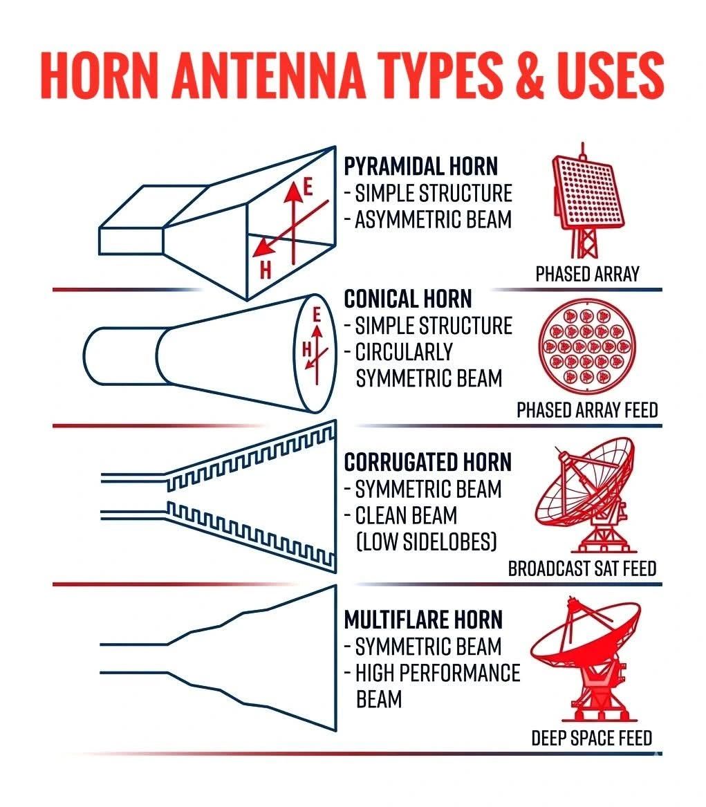
Different horn antennas aren’t just passive components—they’re precision tools for shaping electromagnetic waves in real-world communication systems.
Each design delivers a unique beam pattern tailored to specific applications. Here’s how they compare:
🔹 Pyramidal Horn – Formed by flaring a rectangular waveguide in both directions. Simple, widely used, and ideal for general-purpose microwave work and antenna measurements. The trade-off? The beam isn’t perfectly symmetric.
🔹 Conical Horn – Derived from a circular waveguide, producing a circularly symmetric beam. A top choice in radar systems and standard gain antennas where uniform coverage matters most.
🔹 Corrugated Horn – Internal grooves reduce sidelobes and improve beam symmetry, resulting in a clean radiation pattern. Perfect for satellite communications and high-precision RF systems.
🔹 Multiflare Horn – Engineered with multiple flare angles for superior beam control. Offers excellent symmetry and minimal distortion, making it suitable for advanced applications like deep-space communication.
📡 Where you’ll find them
Horn antennas serve as critical feeds in phased arrays, satellite dishes, and space communication systems—ensuring efficient radiation and precise signal direction over long distances.
Which horn type has been most useful in your RF or antenna work? Let’s discuss below. 👇
#AntennaDesign #RFEngineering #MicrowaveTechnology #SatelliteCommunications #ElectromagneticWaves
English
Designed & Simulated a 50-Ω Microstrip Transmission Line for 5GHz Operation ⚡
In RF engineering, a poorly matched impedance doesn't just degrade performance — it reflects energy back into your source and kills your design.
So I put theory to practice.
Using an FR4 substrate as my foundation, I modeled a microstrip trace geometry optimized for maximum power transfer and minimal signal distortion at 5GHz.
📐 Design Parameters
Substrate: FR4 | εᵣ = 4.4 | h = 1.6mm
Trace Width: 3mm | Trace Length: 8mm
Electrical Length: 90° (Quarter-wavelength) at 5GHz
📊 What the Simulation Revealed
✅ Return Loss (S11) of -35 dB — near-zero reflection, essentially all power delivered to the load
✅ Precise phase control — 8mm physical length dialed in to hit an exact 90° electrical length
✅ E-field visualization confirmed smooth wave propagation and clean electromagnetic energy confinement within the dielectric
The most valuable takeaway? Physical dimensions are not arbitrary — every millimeter shapes how electromagnetic energy travels, bends, and behaves.
Next step: scaling these principles into multi-element feeding networks and antenna arrays.
If you're working in RF, microwave design, or antenna engineering — let's connect. 🚀
#FEngineering #MicrowaveEngineering #AntennaDesign #EMSimulation #5G #SignalIntegrity #EEDesign
English
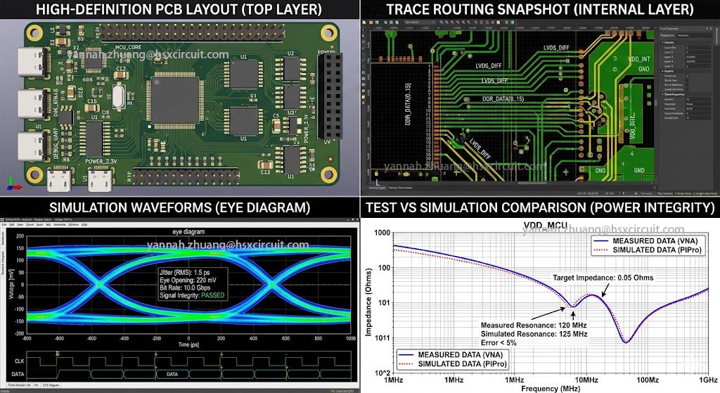
5 Common High-Speed PCB Length Matching Mistakes (That 90% of Engineers Make)
Length matching goes far beyond simply making trace lengths equal — it’s a critical factor in preserving signal integrity.
Here are some frequent pitfalls to watch out for:
1️⃣ Overlooking the return path
Equal trace length doesn’t guarantee equal delay if the reference plane is disrupted.
2️⃣ Excessive serpentine routing
Too-tight serpentine patterns increase crosstalk and cause delay distortion.
3️⃣ Neglecting differential pair skew
The timing difference between pair lines impacts performance more than absolute length.
4️⃣ Over-applying length matching
Not every signal demands strict length control—know when it’s necessary.
5️⃣ Ignoring manufacturing tolerances
Real-world boards often differ from simulation results due to fabrication variations.
Key takeaway: Length matching is a means to an end, not the end itself. The real goal is ensuring robust signal integrity.
What’s the toughest challenge you face when designing high-speed PCBs? Let’s discuss!
English
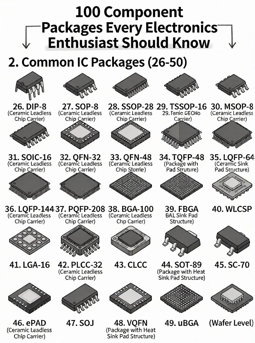
🔧 The package matters just as much as the component itself.
In electronics design and embedded systems, selecting the right IC package can make or break your product — affecting everything from thermal performance and signal integrity to board space and manufacturability.
Whether you're routing a PCB, troubleshooting a hardware issue, or scaling toward production, knowing your packages is a fundamental skill.
📦 From through-hole to advanced surface-mount:
DIP — reliable, breadboard-friendly, easy to prototype
SOP/SOIC — compact, widely supported in SMT lines
QFN — excellent thermal dissipation, minimal footprint
BGA — high pin density for complex, high-performance ICs
This reference covers 26–50 commonly used IC packages, giving engineers and hardware enthusiasts a practical visual guide to recognizing and differentiating them in real-world designs.
💡 If you're growing in electronics, PCB design, or embedded systems — bookmark this. You'll reference it more than you think.
♻️ Repost if you find this useful — let's help the engineering community level up together.
#Electronics #EmbeddedSystems #PCBDesign #HardwareEngineering #EE #CircuitDesign #Engineering
English
Capacitors in Real-Life Circuits ⚡
Continuing my 21-Day Electronics Learning Challenge – today’s focus: how capacitors are actually used in practical applications, beyond textbook theory.
Where capacitors shine in real circuits:
🔹 Power Supply Filtering – smooths voltage and reduces noise
🔹 Coupling – passes AC signals while blocking DC
🔹 Decoupling – stabilizes voltage, especially for ICs
🔹 Timing Circuits – enables delays and oscillators
Real-world examples you’ve likely used:
📱 Mobile chargers → stable DC output
🎧 Audio systems → cleaner sound with less noise
🖥️ Microcontrollers → reliable operation thanks to decoupling capacitors
Key insight:
Capacitors may be small, but they’re essential for building circuits that are reliable, efficient, and noise-free.
Moving from storing charge to improving performance – understanding how components work in real applications makes all the difference.

English
🔍 Microcontroller vs. Microprocessor: Not the same thing.
These terms are often used interchangeably, but they serve very different roles in electronics and embedded systems.
🧠 Microcontroller (MCU)
An all-in-one chip designed for dedicated control tasks.
Includes:
✔ CPU
✔ Memory
✔ I/O peripherals
✔ Timers & communication interfaces
✅ Best for:
→ Embedded systems
→ IoT devices
→ Home appliances
→ Industrial controllers
💻 Microprocessor (MPU)
A CPU-only chip that relies on external memory and peripherals to function.
✅ Best for:
→ Computers & laptops
→ Complex operating systems
→ High-performance applications
→ Advanced processing tasks
📌 Why it matters
Engineers, designers, and sourcing pros: choosing between an MCU and MPU impacts cost, power efficiency, and performance. The right decision early on saves major time and money later.
Which component comparison should I cover next?
#EmbeddedSystems #ElectronicsEngineering #Microcontroller #Microprocessor #ProductDesign #HardwareDesign

English
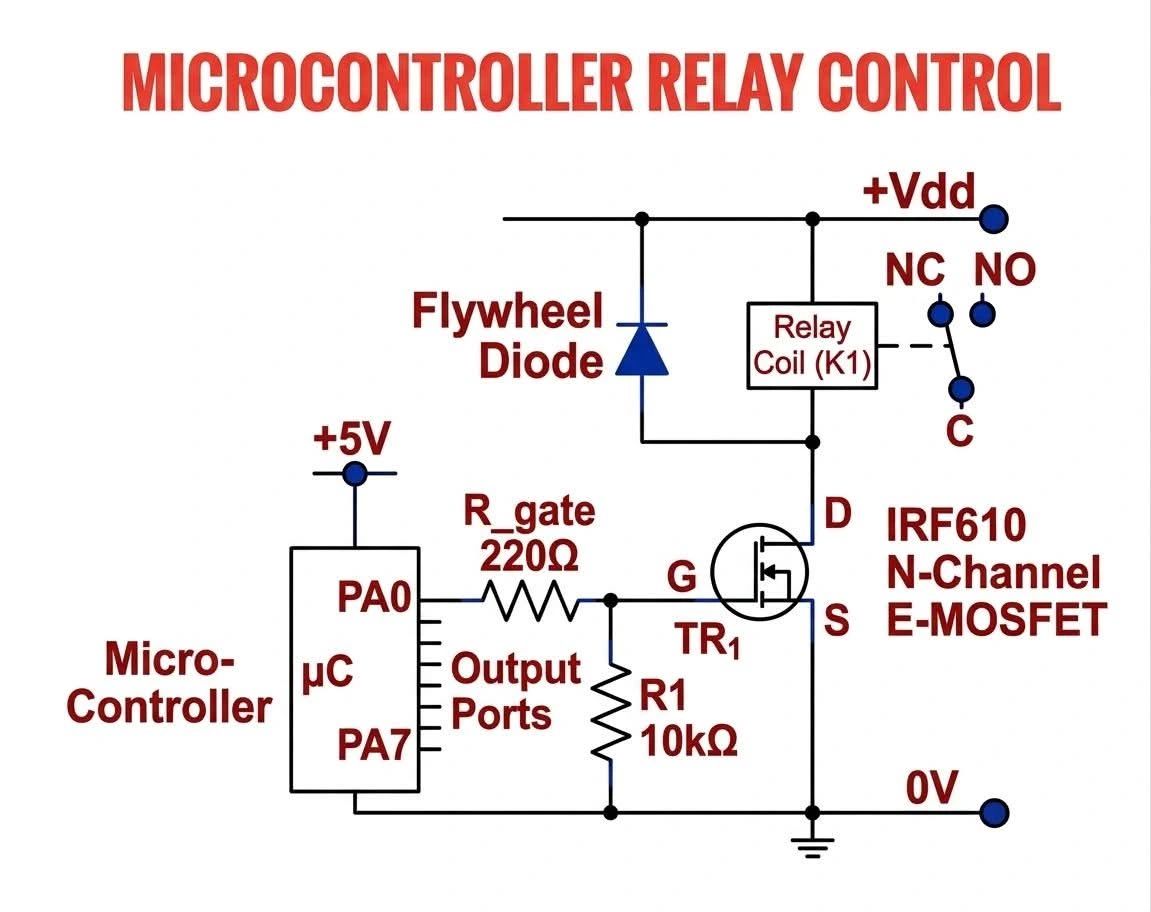
Ever wondered how a microcontroller switches a high-power load without getting fried?
Here's a simple but powerful circuit that does exactly that — using a MOSFET as the bridge between logic and load.
Here's how it works:
When the microcontroller's output pin (PA0) goes HIGH, it triggers the MOSFET gate through a 220Ω resistor. The MOSFET switches ON, completing the path to ground and energizing the relay coil — flipping the contact from NC to NO.
When PA0 goes LOW, the MOSFET cuts off, the coil de-energizes, and the relay snaps back to its default NC state.
Two small components do a lot of the heavy lifting here:
→ A 10kΩ pull-down resistor keeps the MOSFET firmly OFF when no signal is present — no floating pins, no false triggers.
→ A flywheel diode clamps the voltage spike generated when the relay coil collapses — protecting the MOSFET from a potentially damaging kickback.
It's a compact, reliable design that's become a staple in embedded systems — anywhere you need low-power logic to command a high-power world.
Simple concept. Endless applications.
#EmbeddedSystems #Electronics #CircuitDesign #Engineering #Microcontrollers #HardwareEngineering
English
GPUs used to sit on PCBs next to GDDR memory, talking to each other through long board traces.
That worked — until it didn't.
Long interconnects meant high RC delay, limited I/O density, lower bandwidth, and more energy burned per bit. As AI workloads scaled, the architecture hit a wall.
The industry's answer: heterogeneous integration — pulling logic and memory into a single package.
TSMC's Chip-on-Wafer-on-Substrate (CoWoS) is one of the most important enablers of this shift. The idea is straightforward: place the GPU and HBM side-by-side, connect them through a fine-pitch interposer, and eliminate the long PCB traces that were killing performance.
The interposer is the key piece here. It's a high-density wiring layer that enables short die-to-die connections, fine-pitch routing, and bridges chip I/O to the package. Two main flavors exist — silicon (precise, expensive) and organic RDL (cheaper, larger area).
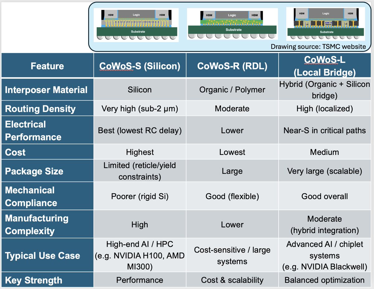
CoWoS comes in three variants, each making a different tradeoff:
CoWoS-S uses a silicon interposer with ~0.5–2 µm routing. Maximum density and performance, but limited by reticle size and cost.
CoWoS-R uses an organic RDL substrate. Lower cost, larger footprint, more flexibility — with some density tradeoff.
CoWoS-L combines an organic base with localized silicon bridges only where high density matters most (think: GPU-to-HBM interface). It's the architecture showing up in large-scale AI systems because it balances performance, cost, and scalability.
The bottom line: CoWoS replaces long PCB interconnects with fine-pitch packaging — and that shift is a big part of why modern AI accelerators can deliver the bandwidth they do.
(Comparison table in the comments.)
#Semiconductors #AdvancedPackaging #CoWoS #HeterogeneousIntegration #Chiplets #AIHardware #HPC #TSMC #HBM #ElectronicsEngineering
English
5 EMI Mistakes Engineers Overlook—Until It’s Too Late
You’ve nailed the PCB design review, but then the EMC test fails. Sound familiar? You’re not alone.
In fact, over 70% of EMI headaches stem from just a handful of preventable mistakes—yet these slip through in real-world projects far too often.
Here are the top 5 EMI pitfalls that can derail your design—and how to avoid them:
❌ 1. Neglecting Return Path Design
Signals don’t just go forward—they return. Interrupting that return path with splits, gaps, or poor layer transitions turns your PCB into an antenna.
Quick fixes:
🔹 Maintain continuous reference planes
🔹 Avoid crossing split planes
🔹 Place stitching vias near transitions
❌ 2. Overlooking Ground Integrity
“All grounds are created equal” is a myth that kills signal integrity. Fragmented or noisy grounds cause unstable references—fueling EMI.
Quick fixes:
🔹 Use solid ground planes
🔹 Keep ground impedance low
🔹 Separate noisy and sensitive zones
❌ 3. Messy Power Distribution Network (PDN)
Your power plane is a hidden culprit. Inadequate decoupling leads to voltage ripple—and unwanted emissions.
Quick fixes:
🔹 Put decoupling capacitors close to IC pins
🔹 Use a mix of capacitor values
🔹 Optimize PDN impedance
❌ 4. Poor High-Speed Routing
Sharp corners, long stubs, and uncontrolled impedance convert traces into unintended antennas.
Quick fixes:
🔹 Control impedance carefully
🔹 Avoid stubs
🔹 Route with smooth, continuous paths
❌ 5. Waiting Too Long to Shield & Filter
Trying to patch EMI issues post-layout? That’s like trying to patch a leaking pipe with tape.
Quick fixes:
🔹 Add filters early—common-mode chokes, ferrites
🔹 Apply shielding where needed
🔹 Consider EMI from day one
A Final Thought
EMI problems aren’t born from complex issues—they’re born from small design slip-ups repeated across the board. Nail the fundamentals, and you can eliminate 80% of EMI risks.
🔁 Your Turn: What EMI challenge has been your toughest to tackle? Share your stories and solutions below!

English