Cardyak

1.1K posts

Cardyak banner
Cardyak

Cardyak

@Cardyak

Computer Programmer/Hardware Enthusiast. #SiliconGang Author of CPU μarch Block Diagrams: https://t.co/TsQtPgYvwW & μarch Cheat Sheet: https://t.co/u17qKZbeRw

Essex, England, UK 🇬🇧 参加日 Ağustos 2009
170 フォロー中1.9K フォロワー
固定されたツイート
Cardyak
Cardyak@Cardyak·
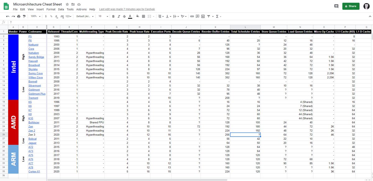
Inspired by @InstLatX64, today I'm introducing the #SiliconGang Microarchitecture Cheat Sheet: bit.ly/2JTplfJ 
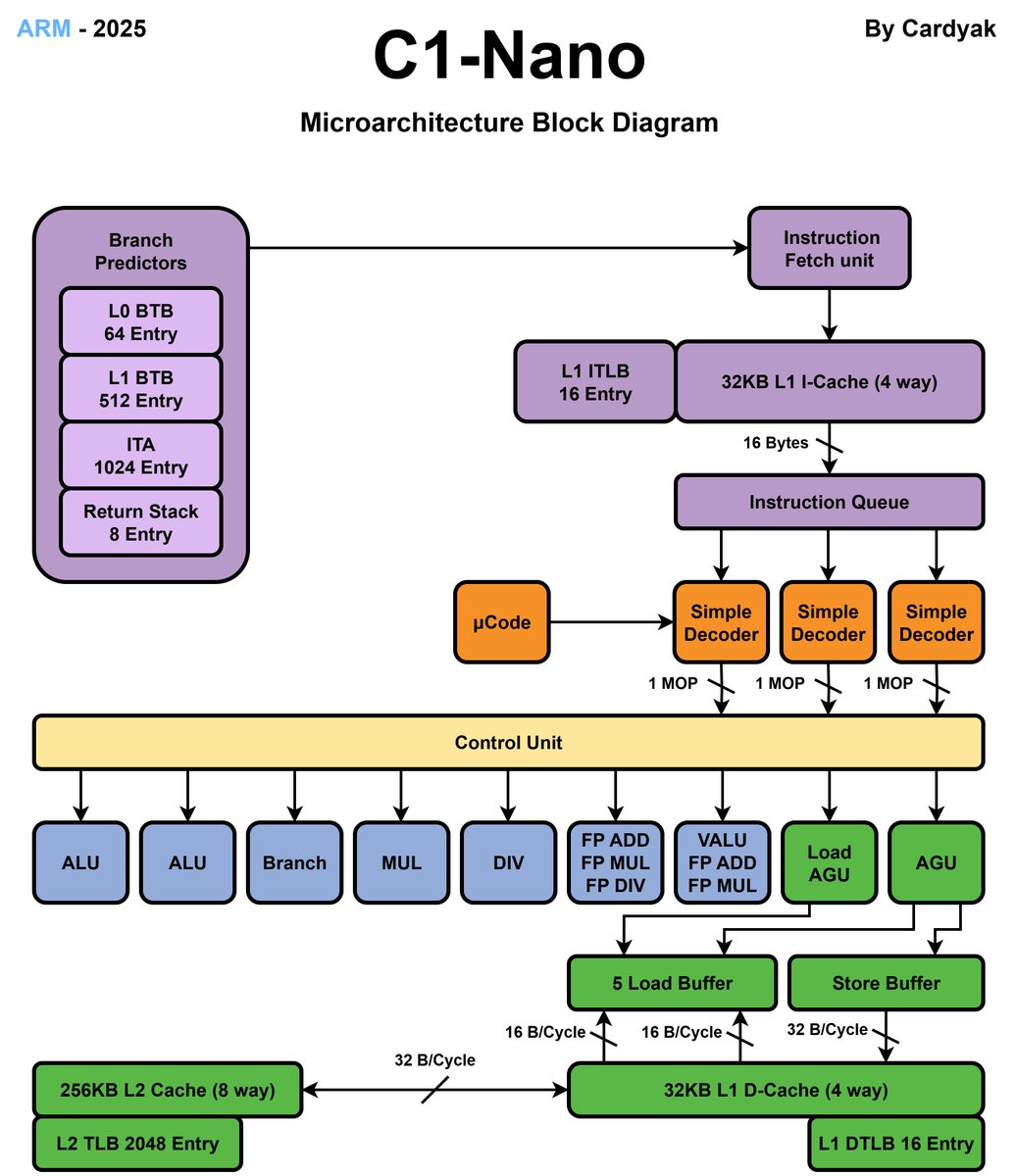
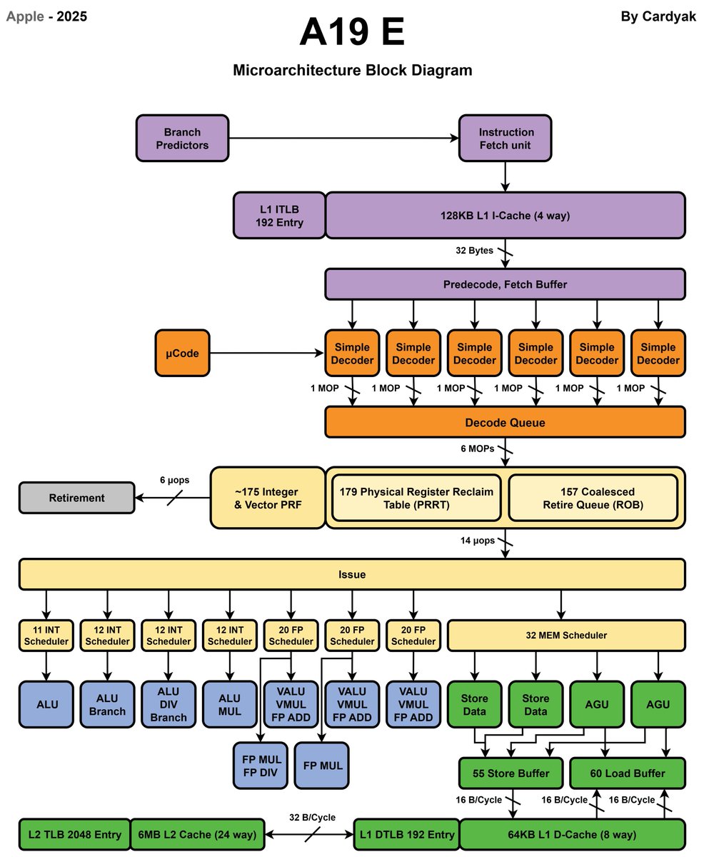
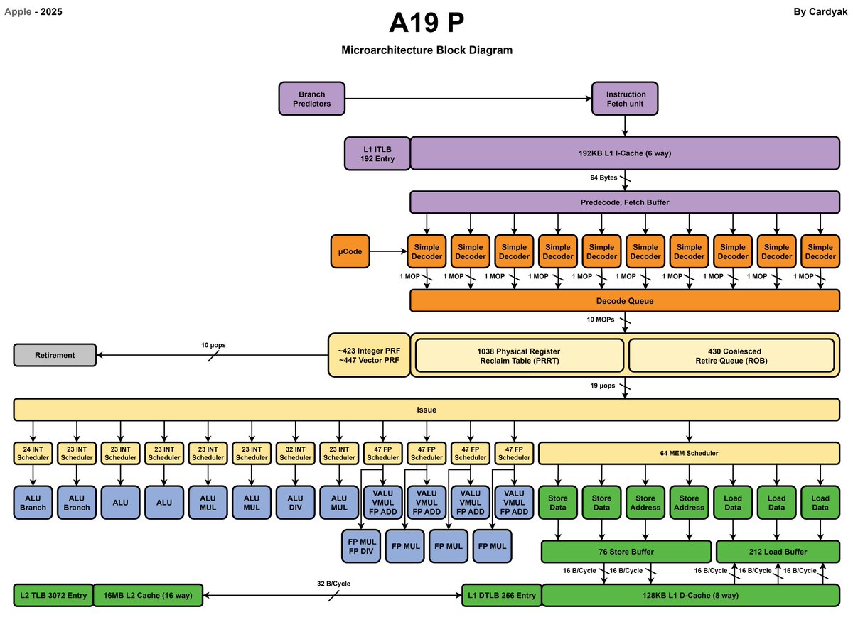
This can be viewed by all, and it offers centralised information about CPU μarch design such as caches, buffers, instruction width, etc. Some notes below:
Cardyak tweet media
English
7
22
94
0
Dylan Patel
Dylan Patel@dylan522p·
$1,000 for whoever comes up with the best name replacement for InferenceMAX InferenceMAX 2.0 dropping soon but we have to rename it because HBO MAX sent us a cease and desist. We have all NVIDIA GPUs from h100 to GB300 on large MoEs with SOTA optimizations like Disagg PD tested
English
366
4
296
59.3K
Cardyak
Cardyak@Cardyak·
dl.acm.org/doi/epdf/10.11… "SHADOW: Simultaneous Multi-Threading Architecture with Asymmetric Threads" "dynamically balances ILP and TLP by executing out-of-order and in-order threads simultaneously on the same core" Could this be what AheadComputing is working on? #CPU #μarch
English
2
4
19
1.9K
Cardyak
Cardyak@Cardyak·
dl.acm.org/doi/epdf/10.11… "ATR: Out-of-Order Register Release Exploiting Atomic Regions" Interesting μarch idea here. Instructions that have finished execution but not been committed yet, and also do not contain conditional branches can free up their PRF entry early #CPU #μarch
English
0
1
20
1.5K
Cardyak
Cardyak@Cardyak·
@OneRaichu Great data! Did you manage to confirm if Darkmont or Cougar Cove and handle 2 taken branches per cycle?
English
1
0
2
316
Cardyak がリツイート
Kurnal
Kurnal@Kurnalsalts·
This Gen Mobile phone SoC size
Kurnal tweet media
English
15
48
899
65.6K
Cardyak がリツイート
Kurnal
Kurnal@Kurnalsalts·
A19Pro with A18Pro area surveying data A19Pro 与A18Pro的面积测绘数据
Kurnal tweet media
中文
3
13
103
24.7K
Cardyak
Cardyak@Cardyak·
@boris_dg N3P only offers a 6% density gain, so by default it’s not enough to shrink down from the size you mentioned to 99mm. There’s more to it than that, especially when you remember the CPU and GPU had extra functionality added which increases the transistor count.
English
1
1
24
2K
Boris G.
Boris G.@boris_dg·
@Cardyak A18 Pro is 109.72 mm² And it's normal to be smaller. It's N3P vs N3E.
English
1
0
4
2.2K
Cardyak
Cardyak@Cardyak·
Apple A19 Pro die shot Die Size 98.68mm² P-Core 2.966mm² P-Core with L2 & Shared Logic 5.486mm² E-Core 0.782mm² E-Core with L2 & Shared Logic 2.217mm² SLC 11.026mm² Somehow looks to be smaller than the A18 Pro (~104mm²) #Apple #iPhone #CPU #A19 tieba.baidu.com/p/10206320725?…
Cardyak tweet media
English
8
70
475
113.3K
Cardyak
Cardyak@Cardyak·
@realnvmd They share cores with the A Series SoCs featured in the iPhone. Firestorm is the M1 big core, A19P is the big core in the M5 as well, etc
English
0
0
0
47
nvmd
nvmd@realnvmd·
@Cardyak Why aren't any of the M series diagrams in the Drive folder?
English
1
0
0
53
Cardyak
Cardyak@Cardyak·
Updated the Apple core diagrams to properly reflect the unconventional ROB structures that are used Still lots of work to do, I need to separate the dispatch queues from the schedulers and research/confirm the L1 ICache bandwidth μarch Block Diagrams: bit.ly/32qLLew
Cardyak tweet mediaCardyak tweet mediaCardyak tweet mediaCardyak tweet media
English
6
24
132
9K
Cardyak
Cardyak@Cardyak·
@MCH2024 There’s also mistakes on their diagram, the ARM documentation tells us there’s 6 FP execution units, not 5. We know this for a fact. Also the ROB increased by up to 25%, so it can’t be above 960
English
2
0
0
396
MCH
MCH@MCH2024·
@Cardyak Geekerwan block diagram is completely different.
MCH tweet media
English
1
0
3
497
Cardyak
Cardyak@Cardyak·
Nice work from @highyieldYT and also @chipwise_tech, wish we had the mm2 measurements to be able to truly compare against the A18 & A18 Pro
High Yield@highyieldYT

.@Apple A19 SoC chip analysis based on images by @chipwise_tech: 2 P-cores with 8MB shared L2$, 4 E-cores with 4MB shared L2$, a 8-core NPU (Apple calls it 16-cores), 2x 6MB System Level Cache (SLC) and a 5-core GPU. All on TSMCs N3P and smaller than the previous A18.

English
0
0
23
2.4K
Cardyak
Cardyak@Cardyak·
@divBy_zero @handleym99 @MrMadbrain Interesting confession! I assume it saved enough area to be worth the compromise? How easily do you think ARM can expand the decode/allocate stage to 12 or even 16 wide?
English
1
0
1
210
Cardyak
Cardyak@Cardyak·
@divBy_zero Would love to see them progress to 12 wide soon
English
1
0
3
320
Eric Quinnell
Eric Quinnell@divBy_zero·
@Cardyak Fixed length isa in the world of llvm and JITs. Burst 10-20 ops and branch. This is the Firestorm gold standard. Until sw changes behavior again, this is how to do it.
English
1
0
2
351
Cardyak
Cardyak@Cardyak·
The IPC for the E Core is so high now, it's only slightly behind the P Core that was present in the A12 (Vortex)
English
0
0
23
1.5K
Cardyak
Cardyak@Cardyak·
Geekerwan's Initial Review of the A19 is out - bilibili.com/video/BV1cBp4z… P Core has ~12% more perf and 6% increase in IPC E Core has ~25% more perf and 17% increase in IPC If these result are accurate then the E core is simply a monster by this point. #iPhone #A19 #CPU #Apple
Cardyak tweet mediaCardyak tweet mediaCardyak tweet mediaCardyak tweet media
English
11
13
184
12.3K
Cardyak
Cardyak@Cardyak·
Looks like Apple’s A19-E Core is 6 wide
Cardyak tweet media
English
2
1
22
4.2K
Cardyak がリツイート
INIYSA
INIYSA@lafaiel·
A19 Pro vs A18 Pro +6.0% better performance per clock vs prev gen
INIYSA tweet media
English
13
33
331
25.5K