Sabitlenmiş Tweet
Alex A.C.
45.9K posts


Alex A.C.
@AnalysisOp
M. Eng. Electronic ⚡ 〰️ Financial data & analysis. Value investing. Growth? at a reasonable price. Jokes (some) are allowed 🦔 🧔🏻
EU Katılım Şubat 2023
139 Takip Edilen2.2K Takipçiler

My friend at NVIDIA told me yesterday that two people from his team recently left.
He is an analog circuit designer, and one person moved to a company that starts with C, while the other moved to a company that starts with A.
Can you guess which companies they joined?
Damnang2@damnang2
Where am I?
English
@ecommerceshares For Tech insights, they are pathetic at the level of talking to a teenager being you an adult with life and experience
English

Looking at these quarterly fund filings for investing ideas is like looking in the rear view mirror while trying to predict where the road is going.
Definitely won’t make you wealthier.
English

Good read
But I don't think we will ever see Mythos or models bigger than that (50T+) on heterogeneous inference hardware
This stack is optimized for sub-5T (tbh even less than 3T) size models
Also, remember that labs are pushing higher token efficiency, so that they don't need to push TPS super hard and can serve at super high batch sizes
But things will change with Feynman and 3D stacking when they can put the memory die on top of the logic die
fin@fi56622380
每年的Nvidia GTC大会,都会带来一些技术范式转新移概念,作为全业界的新技术标杆 各家在GTC之后都会改roadmap去抄作业 总有人问,AI芯片下一波结构性趋势转变的机会在哪里? 这几个月范式转移带来的结构性转变机会之一,就是AI异构推理,而以Cerebras为首的SRAM路线初创,就这样走到了新趋势前沿 ------------------------ SRAM路线的公司生态位在哪里,得先看genAI推理的不同阶段workload特点 主要分成三个部分: prefill:计算强度特别高,对memory带宽速度要求不高,对memory size要求中等偏高 decode阶段的attention部分:计算强度中等,对memory带宽速度要求特别高(对kv cache的反复读写),对memory size要求特别高,因为batch size的变大造成了kv cache的线性增长 decode阶段的FFN部分:计算强度中等,对memory带宽速度要求特别高(模型权重的反复读取),对memory size要求中等偏高(模型权重) SRAM路线的芯片特点也很清楚: 除了memory带宽做到了极致,其他方面都是严重缺陷,本质上是用计算强度和memory size做不大这两个劣势,换取了极致的memory带宽速度 --------------------- 再来分别看AI推理的三个阶段,SRAM的适用度 prefill:SRAM计算强度无法做的很高,因为整个芯片上的SRAM面积占用太大,计算模块面积受限,所以prefill是弱项 decode阶段的attention部分:SRAM memory带宽要求高能达到,但是SRAM memory size很小达不到batch的要求,所以SRAM做attention只能满足一半需求 decode阶段的FFN部分:SRAM memory带宽要求高能达到,memory size要求中等,SRAM芯片通过互联通信的优化,能勉强解决memory size的问题,虽然代价很高,但ROI在某些场景下还是能算的过来的 ---------- 所以SRAM路线的加速器 在AI异构推理的适用范围也很清楚: prefill部分别想了,性能垃圾,经济性垃圾 decode阶段的FFN部分,属于努努力加大成本还能够得着 decode阶段attention部分,kv cache对memory size要求太高,批量处理需求实现过于高昂,让Cerebras昂贵的230万美元一片,45片连成一起的奢侈的一亿美元的系统做成专属的超级VIP服务,完全是经济性灾难 想象一下,一两个用户agent flow做coding任务花了1~2M context length,就得耗费230万美元一整个cerebras的44GB SRAM来做KV cache,不然速度就上不去,这是什么样的奢侈服务 ------------- 所以结论简直不能再明显了:Cerebras如果单独做全栈AI推理(prefill + decode ATTN + decode FFN),经济上是走不通的,没有未来的 因为Cerebras成本是非常惊人的,即便是他们毛利率压的如此之低,每台 CS-3 系统的隐含租金还是要 $41.96/小时,是B200的差不多十倍租金,更不要说CS-3还得很多片连起来做LLM推理,租金要再乘以很多倍。 这也是为什么SRAM路线经济效益如此差的原因,Nvidia在GTC已经清晰的指出了这一点(如图)。 鼓吹SRAM路线以后取代HBM?那是痴人说梦,SRAM的scaling已经撞墙的情况下,每代芯片上的SRAM密度已经很难提升,在memory size这个维度上,HBM的指数型增长只会更加和SRAM拉开差距。即便是memory 带宽这个维度上,HBM也在指数型增长,缩小和SRAM的差距 所以Nvidia的解法非常简洁而优雅:decode阶段的FFN部分交给SRAM路线,其他部分交给传统HBM GPU,把整个pareto frontier往右上角推进了很多 Rubin + LPX最高速度突破1000 token/s的同时,还能让整体throuhput仍然能保持一定的商业价值(这点很重要)。要知道如果在Blackwell要跑到400~500 token/s高速,只能同时处理很少的几个请求,这对GPU资源是巨大的浪费。 而现在就算是跑到1000 token/s,也能保持一定的batch size(吞吐量)了,终于也能产生商业价值了,图里说在400 token/s的速度下,Rubin + LPX把吞吐提升了35倍,就是典型的token经济学,这个token高速度下,从Blackwell算提升了35倍的商业价值 --------------------- 这个解法在GTC公布标准答案之后,甚至更早在收购Groq的LPU之后,大家就已经开始做异构推理这个方向抄作业的努力了 Google的TPU找了Marvell做SRAM部分 Amazon AWS的trainium找了Cerebras做SRAM部分 字节的AI asic找了高通做SRAM部分 未来我们一定会看到越来越多类似的消息 而这就是Cerebras在经济上可持续的最好道路:不要硬扛全栈AI推理,只做自己擅长的部分,在AI推理中和主流AI ASIC合作,争取能把自己SRAM芯片融入其他家的AI推理的decode FFN环节 这也是为什么,Cerebras长期发展的关键在于和aws trainium的disaggregate inference能整合到什么程度 如果只是目前爆出的Trainium做prefill和Cerebras做decode分离,技术上实现难度要小的多,但是这样经济上仍然不划算 ,只能是战略布局,能有一定的市场,但无法真正产生规模化竞争力 而走Nvidia路线,深度整合两家优势,需要不少时间的技术整合,难度不小,但回报是值得的。解法一:trainium做prefill和decode attn,Cerebras做decode FFN。或者解法二:Cerebras做草稿模型,trainium做验证,。无论是哪种解法,市场竞争力都大太多了 -------------------- 和主流AI ASIC这样的合作方式,是减小了SRAM路线的市场规模TAM吗? 不,这才是SRAM路线的公司唯一的长期可持续化增大市场规模的道路,因为AI异构推理趋势一定是未来,提前在这个增长的未来蓝图中找到属于自己的拼图位置,才能跟着市场一起增长 SRAM路线公司一旦融入任何主流AI ASIC的异构推理环节,身价都会暴涨,因为出货量的TAM完全不是一个数量级了 不然的话,AI异构推理在token速度(不是throughput)这个维度上,一定会持续的蚕食SRAM路线的速度优势,SRAM路线AI全栈推理沦为昂贵的玩具是注定的结局
English
@zephyr_z9 "COUPE: All-optical interconnects to replace copper as data centers scale to millions of GPUs and power needs surge 200x"
English
Read this
Dan Nystedt@dnystedt
TSMC 2026 Technology Symposium (Taiwan 5/14) Summary: Global Expansion & Operations · Global Build-out: Constructing or modifying 18 fabs worldwide (includes 5 advanced packaging plants). · Taiwan Core: 12 of these 18 facilities are located in Taiwan. · Acceleration: Expansion speed has doubled to 9 new plants per year (2025–2026) vs. 4 per year (2017–2024). International Site Progress · Arizona (USA): -Fab 1 output to grow 1.8x in 2026. -Fab 2 equipment move-in 2H-2026 (N3 production 2H-2027). -Fab 3 broke ground 1H-2025. -Fab 4 and first advanced packaging plant (AP1) are in initial construction. · Kumamoto (Japan): -Fab 1 (28/22nm) yield already equals Taiwan levels; 2026 output target is 2.3x YoY. -Fab 2 began construction in 2025 for N3 production. · Dresden (Germany): -ESMC facility focusing on 12nm–28nm for Automotive/Industrial. Advanced Process Roadmap (N2 / A14 / A12) · N2 Momentum: Fab 20 (Hsinchu) and Fab 22 (Kaohsiung) are in mass production. Taichung Fab 25 to follow in 2028. · N2 Performance: First-year output expected to be 45% higher than N3's first year. Capacity expansion CAGR of 70% seen 2026–2028. · Yield Maturity: N2 yield learning curve is 2 quarters ahead of N3 at the same stage, driven by AI-optimized manufacturing. · A14 (1.4nm): Already achieved >80% yield on 256Mb SRAM; offers 10–15% speed boost or 25–30% power reduction vs. N2. · New Nodes: -A12 (Performance-focused with Backside Power/Super Power Rail) and A13 both targeting 2029 production. -N2U(enhanced 2nm) slated for 2028. · Next-Gen: CFET architecture reduces SRAM cell area by 30%vs. Nanosheet. Advanced Packaging & Silicon Photonics · CoWoS Scale: 5.5x reticle size now at 98% yield. Scaling to 14x reticle for 20 HBMs by 2028 and 24 HBMs by 2029. · System on Wafer (SoW): Future "Super Exchange" chips to integrate 64 HBMs/16 CoWoS units, exceeding 40x reticle size with 100TB+ bandwidth. · Growth: 3DIC/CoWoS capacity CAGR of >80% 2022–2027. · COUPE: All-optical interconnects to replace copper as data centers scale to millions of GPUs and power needs surge 200x. Specialty & Memory Shift · The Memory Divorce: Shifting from eFlash to RRAM (ReRAM) and MRAM for advanced nodes (≤28nm) in Auto, AI Glasses, and Edge AI. · Edge AI Specs: -N4PRF (RF process) for 39% power reduction -N16HV(16nm High Voltage) specifically for AI Smart Glasses/AR displays. $TSM $NVDA $AAPL $AMD $AVGO $MRVL $INTC $AMZN $GOOGL $MSFT $META #semiconductors Links: news.cnyes.com/news/id/6458515 cna.com.tw/news/afe/20260… ctee.com.tw/news/202605147… money.udn.com/money/story/56…
English
@BSkypia59338 obviously top management are so giga arrogant and out of touch with reality
English

와....
삼성전자 사내게시판에
국민여러분께 사과드린다는 공지가 떴다.
삼성전자 직원 외에는 볼 수 없는 게시판에
직원들에게 죄송하다고 하는 것이 아니라
'국민' 들에게 사과를 드린덴다.
그리고 자연스럽게 5분귀 한국경제를 시작으로
속보를 내놓고 있다..ㅋㅋㅋㅋㅋㅋ
이러고 또 정부랑 사람들은 귀족노조니 뭐 어쩌구 하겠지ㅋㅋㅋㅋㅋㅋㅋㅋ
긴급조정을 위한 밑밥이면서
가처분 신청에 대한 명분 쌓기.
진짜 정내미가 떨어지네
한국어

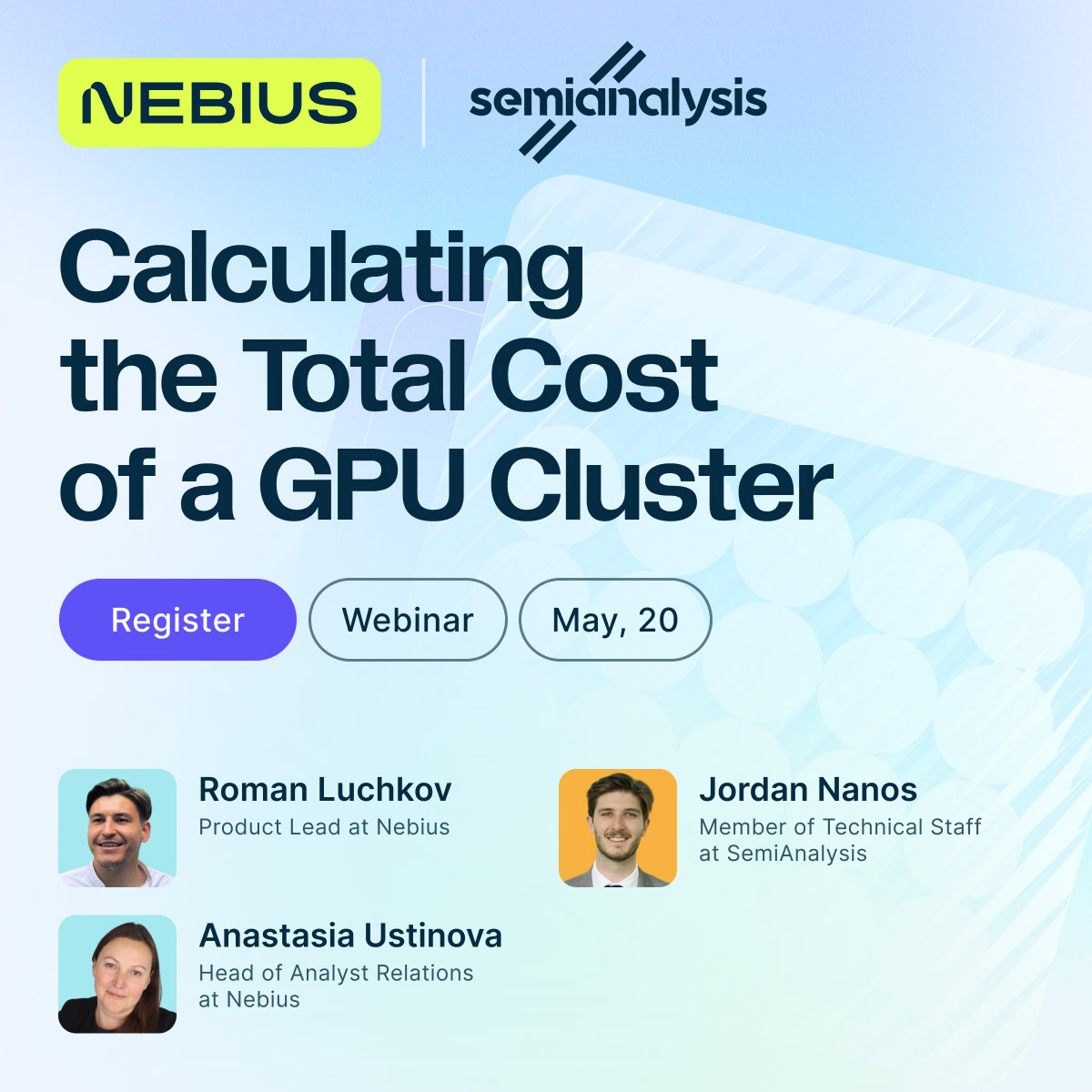
Join Nebius + SemiAnalysis for a technical deep dive into what really determines GPU infrastructure efficiency in production.
May 20 at 9 AM PT / 6 PM CEST
If you’re evaluating infrastructure for training or inference workloads, this session will give you a more defensible way to compare providers beyond GPU-hour pricing.
Register here: nebius.com/events/webinar…
English
The Japanese " $SNDK " soon in the US Market 🇺🇸🇯🇵
NAND demand and pricing is 🚀🪐
Dan Nystedt@dnystedt
Kioxia, the Japanese NAND Flash memory chip giant, plans to list shares on a U.S. stock exchange “to grow its investor base and increase its corporate value,” the company said, noting details of the planned ADS listing, including which market, have not yet been decided. $MU $HXSCL $SSNLF #Kioxia $285A #semiconductors #semiconductor kioxia-holdings.com/en-jp/ir.html
English

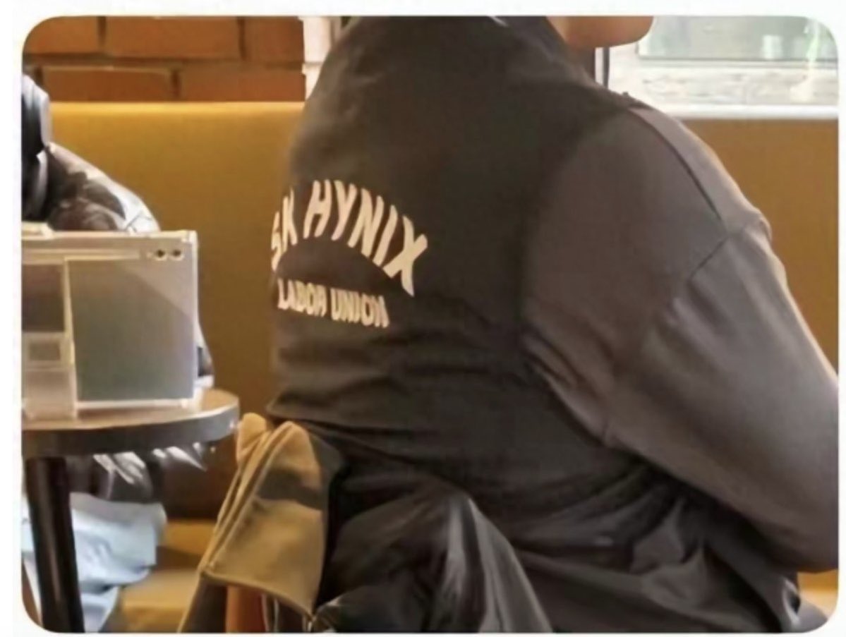
According to South Korean media reports, employees of SK hynix are now becoming some of the most sought-after people in the matchmaking market in Korea 🇰🇷.
In the past, the most desirable matches were usually lawyers, doctors, professors from top universities, or executives at major corporations.
Now, if an SK hynix employee shows up at a matchmaking event wearing a company uniform, they may immediately attract intense attention from a crowd of attractive and highly educated women, all competing for a chance to date — and eventually marry them.
English
@PhotonCap Not AEHR, but I finally surrender and bought SOI 😊 Still at a not-crazy P/S and all the PICs in the world will need a SOI substrate, is mounted on Si or glass substrate.
And "trillions" of PICs will be manufectured.
English

@demian_ai We've public libraries for hundred of years (in Spain started Gov. campaigns in mid XIX century),and now for 25 years a lot of knowledge at a key (from the keyboard) of distance, and... what ppl. do? Read less than ever and use their supercomputers (smartphones) to write nonsense
English

In a world of infinite, free answers, the question is the only remaining differentiator.
Gurwinder@G_S_Bhogal
Picasso’s reply when asked for his thoughts on computers in 1964 is more relevant than ever:
English
@zephyr_z9 I'm not playing this game thx. A lot of names out there
English
Btw, the first qualified partner for Nvidia and most ODMs/OEMs for SSTs is Delta electronics
Play wisely
Irrational Analysis@insane_analyst
15+ people have pinged me in $ENPH and $SEDG and... I hate to admit it but its not completely stupid. Dead home solar stocks pivoting to solid state transformers... is credible. Very degen play to be clear. Each is only 1% of trading account.
English
@BorjaBarba solo les queda devolvernos toneladas de plata saqueada, decenas (o cientos) de cuadros del más alto nivel, devolver la vida a decenas de miles genocidados (civiles), y restaurar los cientos de edificios históricos destruidos... en una guerra ilegal (la invasión fue a traición)🇫🇷
Español

@ShawarmaCapital Let's hope those final certifications are confirmed, or a new contract is announced👌
I understand the big guys of the management didn't go public to wait for 24 months for the certification having only $$$ to hold for 18 months
English


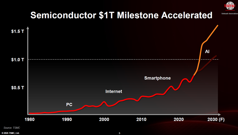
What the...
The $1 Trillion semiconductor TAM was supposed to arrive in 2030. It just got pulled in to 2026.
The new 2030 TAM? $1.5 Trillion. 50% higher than the original ceiling.
Chips are not eating the world. They already ate it.
$MU $SNDK $DRAM $TSM $NVDA $INTC $AMD
English
"If $GOOGL TPU v9 upgrades the topology [potentially a 6D torus] a 4x increase in ICI bandwidth [it's possible].
If coherent optics [are introduced], dollar content per optical module could x2.
Upstream components (lasers, modulators, PICs, DSPs, connectors...) will benefit"
FundaAI@FundaAI
From some discussions we came across today on TPU v9 networking, the direction seems broadly consistent with what we had touched on in our earlier report. The next step-up in Google's TPU networking bandwidth appears to come from two directions. First, the new scale-out network architecture, which seems to be increasingly corroborated by the Boardfly direction and Virgo Network. Second, the continued upgrades in scale-up / ICI bandwidth. We had also flagged the possibility that future TPU systems could move toward a higher-dimensional torus topology, potentially a 6D torus. If TPU v9 upgrades the topology, optical module speed, and port ratio at the same time, a roughly 4x increase in ICI bandwidth versus TPU v8 may not be entirely out of reach. This is likely not just a matter of "buying more optical modules." It could reflect a system-level architecture shift in Google's TPU roadmap toward higher bandwidth and higher optical interconnect content. One point that did not get much airtime in today's discussion, but which we had spent more time on in our earlier report, is the potential introduction of coherent-lite technology. If coherent optics does make its way into this part of the architecture, the dollar content per optical module could rise meaningfully — in some designs, perhaps even close to doubling. It would also bring in a more complex modulation stack, which may call for more advanced silicon photonics, thin-film lithium niobate, or other higher-end PIC platforms. That matters because the value migration would not be limited to the module layer. It could also benefit upstream components, including lasers, modulators, PICs, DSPs, connectors, and advanced packaging. If this plays out, the TPU networking upgrade would meaningfully shift more AI cluster value into optical and connectivity content. Names we'd keep an eye on as potential beneficiaries include $LITE , $COHR , InnoLight, $NOK , $MRVL , $SMTC , $AXTI , and $TSEM .
English
@trendforce "Because the company’s semiconductor fabs are already highly automated..."
Company says that to customers to calm them down 😂😂
English

Samsung’s strike is set to formally begin on May 21. Because the company’s semiconductor fabs are already highly automated, the impact on production is expected to be limited. However, there will likely be noticeable disruptions to packaging and logistics, R&D and design, as well as customer relations. In terms of unionization, about half of all employees across the Samsung Group are union members, most of whom work in the semiconductor division. Internally, management has already extended an olive branch to the DRAM division, but has not yet reached an agreement with union members in the Foundry and LSI divisions.
Reuters@Reuters
Samsung Electronics and its union failed to reach a pay deal, raising the risk of a strike that could disrupt chip production. South Korea's prime minister called for more dialogue as authorities monitor the situation to prevent a strike reut.rs/4wvJUSo
English
$TSM System-on-Wafer (SoW). The future is BIG 😉 (and it will be able to carry a lot of memory)
Trade Whisperer@TradexWhisperer
$MU $DRAM $TSM Holy Shit 2026: 12 HBM stacks per substrate 2029: 64 HBM stacks with SoW That is a 5x structural expansion of HBM demand per system. The memory content per platform is not peaking. It is just getting started.
English
@BSkypia59338 So the PIC uses a SOI yes or yes, and then can be attached to a Si or a glass substrate ? Correct?
English
유리기판이랑 SOI Wafer랑은 좀 다른 얘기에요.
PIC(SOI) + EIC(Bulk) 붙인걸 보통 Optical Engine 이라고 하고 이걸 base 기판 (아래 이미지에서는 interposer)에 붙이는데,이 base 기판을 유리로 하냐 실리콘으로 하냐가 말씀하신 유리 기판에 대한 부분입니다.
요즘 PIC는 무조건 SOI Wafer를 사용하고 있습니다

한국어