Sabitlenmiş Tweet

Well, that's likely it, for the foreseeable future I'm retired as a content creator!
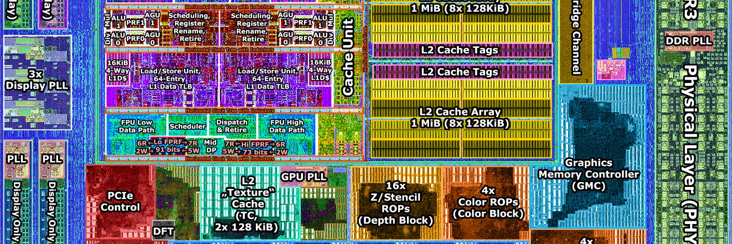
My last analysis goes over the area breakdown of N31 and AD102/103, looks at very rough cost estimates for the chips and perf/mm².
YT:
youtube.com/watch?v=D34qur…
Substack:
locuza.substack.com/p/radeon-n31-v…

YouTube

テカナリエ清水@techanalye1
NVIDIA AD103 NVIDIA AD102
English