Sabitlenmiş Tweet

I'm currently overweight in Space, memory, Energy and Materials going into 2026 and to 2030.
English
Michael Frank Reichmann
273 posts
@MikeFReichmann
AI Enthusiast | Macro & Market Commentist


feels like one of those days where #BTC strength keeps $IREN flat for the day until BTC naturally cools off towards the end of the day and IREN will -4% on the cool off after ignoring the $70k break.
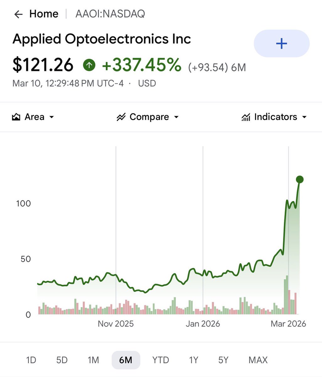
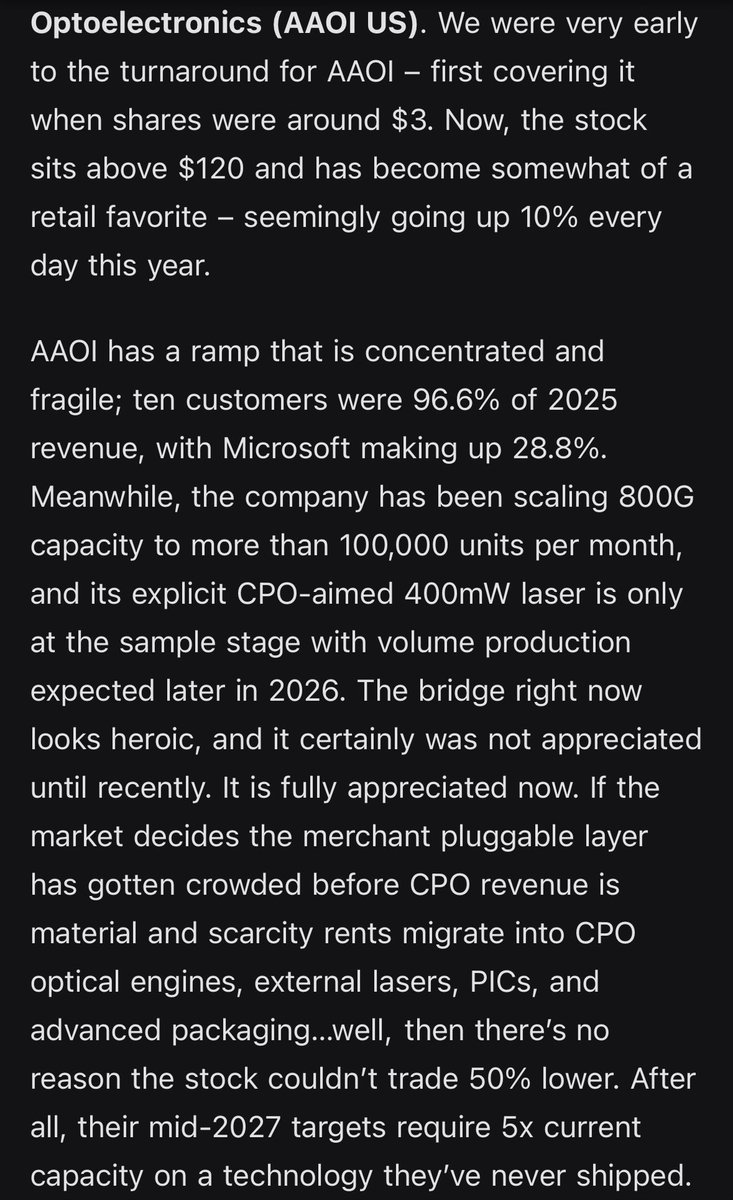
$AAOI is up 24% and $LITE is 5% since my thesis today. From BOM analysis, LITE ($27B) is levered toward TPU Ironwood due to OCS but benefits from NVDA + all ASICs. AAOI ($2.5B), is levered toward MSFT MAIA ramp and Amazon Trainium. InP like HBM, will be a bottleneck for 2026 as they’re the foundational materials used for lasers in these deployments. Similar to memory bottlenecks with Micron and SK Hynix, we’ll likely see attention drawn to InP fabs, such as $AAOI, which happens to be one of the sole ones in America (COHR,Macom) But compared to $LITE that is up 362% YTD due to the success of Google’s TPU (from Meta and Anthropic purchase orders), $AAOI is only up 7% YTD. We’re largely seeing this because there’s a lack of retail or media attention on the $AMZN Trainium or $MSFT Maia deployments, which are largely expected to ramp up in 2026-2027. However they’re all likely to succeed due to each hyperscaler wanting to lower costs of inference for their own cloud platform. If we see other hyperscalers adopt OCS for optimized performance that the TPU achieved, expect $LITE to re-rate more than they have now given their monopoly in that specific segment. However, if we see $MSFT Maia ramp up (given $AAOI is likely developing a new architecture for them), and $AMZN Trainium ramp up ($4B warrant + purchase orders), expect $AAOI to rerate. Photonics and InP will be the new bottleneck like memory. We’ll likely see investments pour down stream to players like $COHR, Innolight, $LITE, and hidden levered plays on specific hyperscaler ASICs like $AAOI as a theme in 2026. The market is currently rewarding the Google TPU supply chain but might be missing other hyperscaler ASIC ramps.
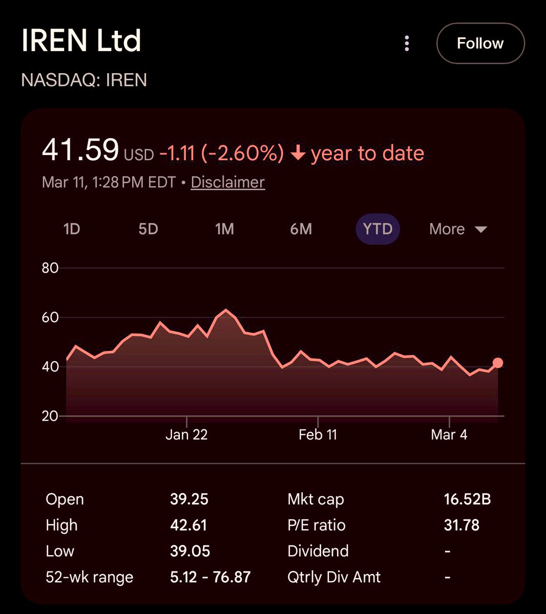
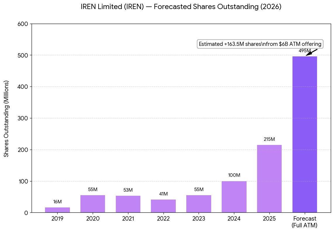
$IREN $6 Billion ATM is massive. For the people who hold $IREN, the truth you might not want to hear is: -> Wait until existing holders get diluted to oblivion -> Use them to "buy the dip" of $6 Billion in new shares for you. -> Go long after. If you're long now: That inevitable $6B in new shares + selling pressure structurally caps upside in your equity and serves as a overhang in any rally. Companies don’t file a $6B ATM not to use it. They will, and as much as they can on any rally. The reality is that there are other financing methods, but ATMs are the most destructive ones to retail shareholders. $IREN itself is a solid company unlike movie theater stocks, but like excessive dilution referenced: You will likely see the marketcap of $IREN go up back toward $20B, but the your share prices tanking in value. TLDR: The harsh reality is $IREN might fundamentally succeed and build a massive DC footprint. But it's at the cost of heavily diluting retail shareholders. Retail investors should care more about the value of their own stock increasing over the company's value. Disclosure: I have zero economic interest or positions in the company, but I do care about prioritizing retail interest.


$IREN is cooked...


Oh forgot about a potential negative catalyst: $AVGO ER 😓


Understanding Scale-Up vs Scale-Out CPO 📓 $LITE $COHR $AAOI $MRVL $POET Yesterday I talked about how the optical supply chain is effectively sold out. But to understand where this industry goes next, we need to understand where optics actually sits inside an AI data center. Right now it is easy to mix up two completely different conversations: Scale-out networking vs Scale-up networking. And they have very different implications for optics investors. Think about an AI data center as three different networks, each operating at different distances. 1) Scale-Across This connects entire data center buildings or campuses. This layer has been optical for years. 2) Scale-Out This connects racks of GPUs across a cluster. This is the network that allows thousands of accelerators to communicate with each other. This layer already runs primarily on optical networking, using pluggable transceivers like 800G and soon enough 1.6T. As $COHR CEO Jim Anderson explained when discussing the architecture of AI clusters: “pluggable transceivers will remain the dominant form factor in, certainly in scale-across and in the scale-out networks, through at least the rest of this decade.” Large AI clusters require enormous east-west bandwidth, which drives a massive number of optical links between racks. 3) Scale-Up This is the shortest network. It connects GPUs inside the same rack. Today this layer is dominated by copper cables (DAC). That’s why Broadcom CEO Hock Tan recently said: “I'm talking about scaling up in a rack... You really want to use Direct Attach Copper as long as you can.” At very short distances copper still wins on cost, latency and power. But this point is crucial. When companies talk about CPO (Co-Packaged Optics) they are referring to two different architectural transitions. The first is Scale-Out CPO, which moves optics closer to the switch ASIC. Scale-out networking already relies heavily on optics today. Early scale-out CPO changes how optics are packaged and integrated. As $LITE CEO Michael Hurlston explained at Morgan Stanley: “In the scale out, we’re cannibalizing ourselves as an industry.” Some links that previously used pluggable transceivers may migrate toward optical engines or ELS architectures. The traffic itself already travels over optical links. I like to think of CPO inclusion here being a necessary proving point on the journey to scale-up. This is why optical demand continues accelerating even while the architecture evolves. $COHR management described the demand environment: “we experienced another step function increase in our data center bookings, with a book-to-bill ratio that exceeded 4x.” Customers are placing orders years in advance to secure supply. Now, the second transition is Scale-Up CPO, and this is the larger shift. Here optics replaces copper interconnects inside the rack, including DAC and other short-reach electrical links between accelerators. This introduces an entirely new layer of optical demand. Again from Hurlston: “Scale up is huge... This is all of the back plane of a rack that eventually you're gonna see more and more optics creep into that rack.” Today that network runs on copper. Optical interconnects inside the rack would expand the optical footprint of AI infrastructure significantly. Like, really significantly. This explains why the industry conversation sometimes sounds contradictory. Broadcom emphasizes copper efficiency inside the rack. At the same time optical suppliers report record demand and multi-year backlogs. Both observations reflect different parts of the same architecture. And both copper and optics are seeing massive surges as more and more data centers are being built. The current optical ramp is primarily scale-out networking. That is why companies like $LITE $COHR $AAOI are experiencing explosive demand. Hyperscalers are building massive AI clusters that require tens of thousands of optical links between racks. Even without optics inside the rack yet, the scale-out network alone creates extraordinary demand. And the major constraint centers on lasers. As Hurlston said while discussing NVIDIA’s investment in the supply chain: “They’ve locked up... a significant amount of the world’s capacity of indium phosphide.” Hyperscalers are securing laser supply years in advance. So the key takeaway is that the optical boom happening today already reflects the enormous scale of AI scale-out networking. If optical interconnects expand inside the rack as well, the optical footprint of AI infrastructure grows dramatically. That is when the real supercycle begins. When? No one knows. But we have an idea and there will be signs. In my next post I will dive into: • Why Scale-Out CPO reshuffles value in the supply chain • Why Scale-Up CPO expands optical TAM • What this means for pluggables vs copper • Which companies are best positioned Disclaimer: This is for educational purposes and is not investment advice.
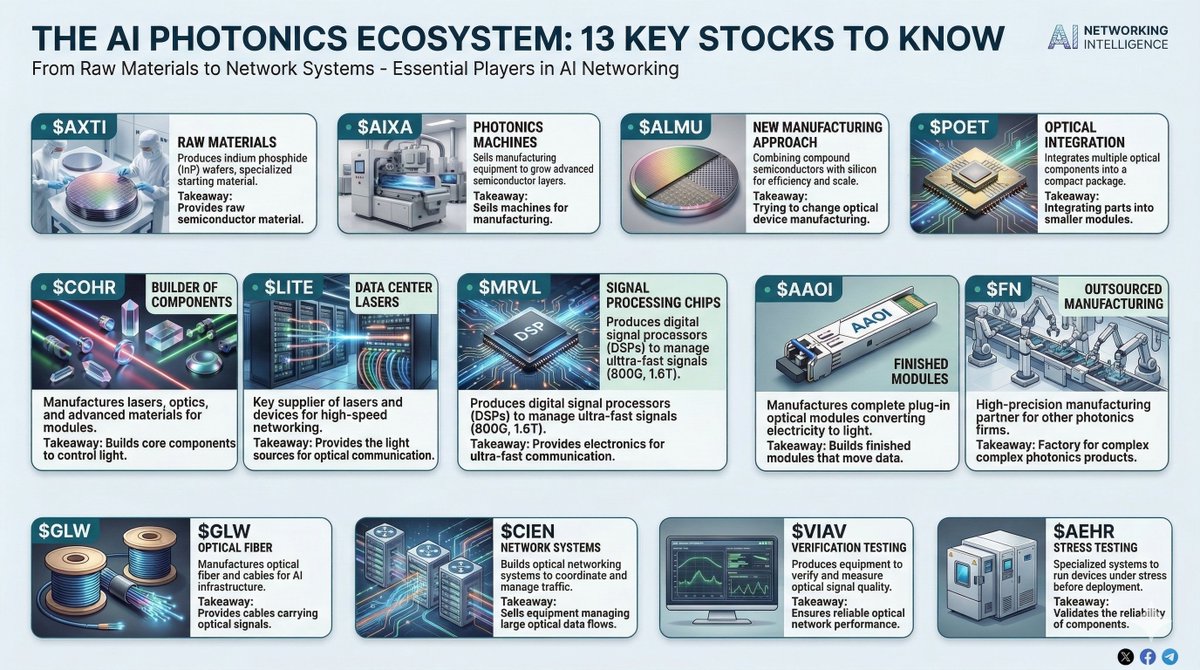
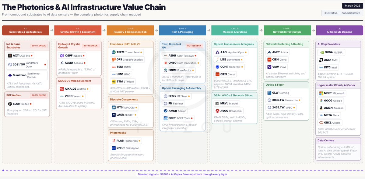
Education Saturday! 📓 For all my Photonics followers, you'll want to learn this $AXTI $LITE $COHR $GLW $POET etc. The Photonics Supply Chain: Start to Finish. Step 0: Mining and Refining It starts with a metal called indium. Indium is what makes high-performance data center lasers possible today. Without it, you can't build the components that move data at the speeds AI demands. Indium has no dedicated mines. It doesn't get extracted on its own. It's a byproduct of zinc refining, meaning it only gets recovered when zinc smelters have the equipment and economic incentive to capture it from their waste. Step 1: The Substrate Refined indium gets combined with phosphorus to create a material called Indium Phosphide, or InP. InP has a unique property in that it can generate light directly from electricity. Silicon, the material that runs everything else in computing, cannot do this. That's why InP is the go to for the lasers inside data center optical components. The first thing you make with InP is a wafer which is a thin, flat disc that serves as the foundation for everything built on top of it. InP wafers are expensive, brittle, and difficult to produce at large sizes. The industry is only now moving to 6-inch wafers. For context, standard silicon chip fabs run on 12-inch wafers. That size gap is a big part of why photonics capacity is so hard to scale quickly. Step 2: Epitaxial Growth A bare InP wafer still can't do anything useful. To create a laser, you have to grow extremely thin additional layers on top of it, each just a few nanometers thick (a human hair is roughly 80,000 nanometers wide). This process is called epitaxy. The exact chemical composition of each layer determines the laser's wavelength, power, and efficiency. Get it slightly wrong and the entire wafer is scrapped. This step requires specialized equipment found in very few places in the world. It's rarely talked about, but it's one of the most critical bottlenecks in the entire supply chain. Step 3: Wafer Fabrication Now the actual circuit gets built. Using techniques similar to semiconductor chip manufacturing (patterning, etching, depositing materials etc.) engineers carve microscopic structures into the wafer: the channels that guide light (called waveguides), the cavities where light gets amplified, and the components that switch it on and off. Unlike standard chip manufacturing, at this time this cannot be done in a regular semiconductor fab. It requires a dedicated photonics facility. These take years to build, qualify, and ramp. There are very few of them in the world. Step 4: Dicing and Yield The finished wafer gets cut into individual chips. Each chip is then tested to see if it actually works to spec. The percentage that pass is called yield and it's one of the most important numbers in this business. Low yield means high cost per working chip. Improving yield is one of the biggest levers on profitability, and it's hard-won through years of process refinement. You probably won't see it reported directly, but it's hiding inside gross margins. Step 5: Component Assembly A working laser chip still can't be used on its own. It has to be physically aligned to an optical fiber with tolerances finer than a fraction of a micron and combined with other components like light detectors and signal modulators to create a functional optical sub-assembly. Automating it reliably at high volume remains one of the hardest manufacturing problems in the industry. The assembled component also has to be hermetically sealed inside a protective ceramic and metal enclosure. Data centers run hot, and moisture or dust will degrade a laser chip quickly. These hermetic packages are specialty components with few suppliers and long lead times and they have shown up as a bottleneck alongside InP when demand spikes. Step 6: The Transceiver Module The optical sub-assembly goes into a housing along with a DSP chip (a processor that cleans up and interprets the light-based signals) plus a circuit board and casing. The result is a pluggable transceiver: the finished module that slots into a switch or server in a data center. These individually get tested before it ships. That testing process is slow and expensive, and it's a hidden constraint on how fast output can actually scale. Note, in the world of CPO this will change. Step 7: Into the Data Center It plugs into a port on a network switch inside the data center, the hardware that routes data between thousands of servers. And none of it moves an inch without the fiber it runs through. Ultra-pure glass strands, thinner than a human hair, carrying light signals between every switch, server, and building. Follow stocks in this space? Drop a ticker below and I'll tell you exactly where they sit in the stack 👇
I've got lots of thoughts on $AVGO earnings From the perspective of a photonics investor I hope the market sells optics names tomorrow on this read and creates a buy op I am really busy today and tomorrow but ill try to get a post out for you guys sometime mid-day tomorrow Would also like to cover $CIEN and $MRVL earnings in a timely manner if I get the chance Once the substack is launched I will have the ability to prioritize this coverage for a more timely report!