Statera
461 posts


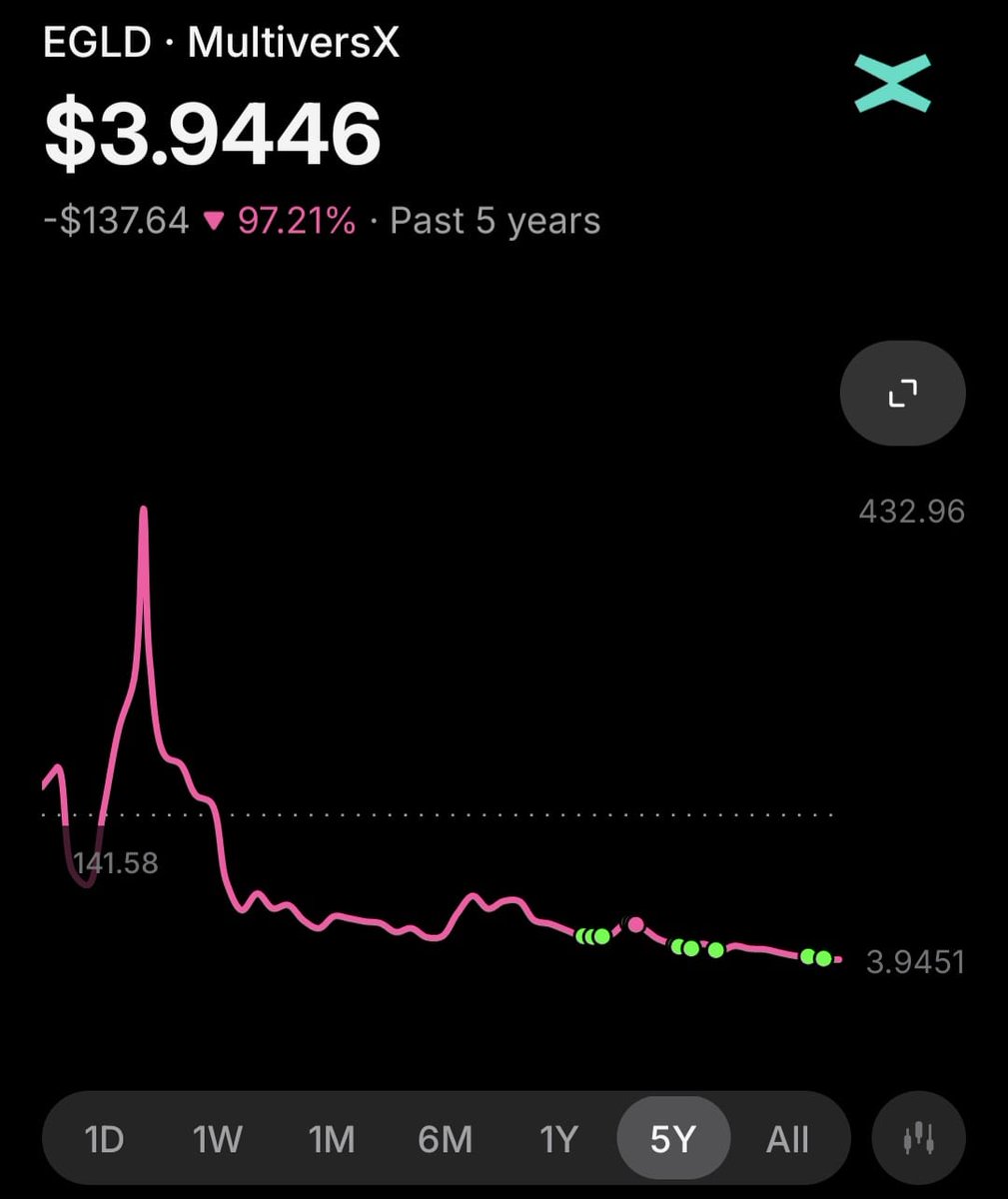
A Bet We Made in 2018 This is me and Vitalik in 2018. ETH Devcon. We were at a table talking about sharding and how blockchains could actually scale by running execution in parallel. At the time, Ethereum and Elrond had the same thesis. Both believed execution sharding was the path forward. Since then, Ethereum changed direction multiple times. Sharding gave way to rollups. Rollups gave way to "we need to scale L1 again." The roadmap shifted, the promises changed, the technical approach pivoted more than once. And through all of it - the Ethereum community stayed. They gave the team the space to find the right path. They didn't kill the project when the roadmap changed. They believed the builders would figure it out. That patience is what kept Ethereum alive. Not the technology. The community. ─── We made a different bet. We bet on execution sharding from day one and we never left that path. Adaptive state sharding shipped on mainnet in 2020. Three execution shards plus a metachain. State, network, transactions - all sharded from genesis. Supernova shipped this year. Consensus decoupled from execution. 600ms blocks. achieved 88ms finality. 120,000 TPS burst mode on the same validator hardware. 3,200+ validators on consumer-grade machines. 171,000 commits. #6 in the entire industry. Ahead of Solana, Avalanche, Sui, Polygon, Aptos, and TON. Tier-one infrastructure providers on board, distribution partners like Cointelegraph are running validator nodes. Stripe's Machine Payments Protocol is settling on MultiversX. EGLD is named in an Arizona state strategic reserve bill. The agentic commerce stack - x402, MPP, MX-8004, UCP, ACP, MCP - is live on one chain. xMoney is building regulated stablecoin issuance under MiCA. The infrastructure underneath has never been stronger. ─── And yet the market prices EGLD like none of this exists. Every blockchain community is going through the same thing right now. EGLD is down. ETH is down. SOL is down. The market doesn't differentiate between chains that shipped paradigm-shifting infrastructure and chains that shipped a landing page. But here's what's different about right now. Bitcoin survived 2014. Ethereum survived 2018. Solana survived 2022. In each case, the community stayed long enough for the technology to matter. In each case, the community that held wrote the next chapter. And in each case, the ones who fractured, who turned on their own builders, who let the loudest voices - the ones who already sold - define the narrative? Those communities don't exist anymore. You don't remember their names. The perception of value has been distorted. By cycles. By speculation. By narratives that reward noise over engineering. And by us - divided when we should be united. Turning on each other instead of building forward together. Look at what's underneath. Not the chart. The infrastructure. 88ms finality. 120K TPS. #6 in developer activity globally. Tier-one infrastructure partners. Stripe settling on-chain. EGLD in US state legislation. Regulated stablecoins under MiCA. An agentic commerce stack that Visa, Coinbase, and Mastercard are racing to replicate. This is not a project searching for relevance. This is a project that shipped the relevance and is waiting for its community to match it. If this fails, it won't be because the technology wasn't good enough. It will be because we weren't united enough to carry it forward. I've been here since 2018. That table with Vitalik. Every pivot, every cycle, every doubt. Still here. Still building. Now it's your turn. Not to believe. To show up.


🇺🇸🇮🇷 U.S. and Israel just struck Iran. World leaders are reacting. Some allies are condemning it. EU leaders Costa and von der Leyen: "greatly concerning," urged restraint and respect for international law. France's Macron: "Outbreak of war between US, Israel, and Iran carries grave consequences. The escalation is dangerous. It must stop." Spain's Sánchez: "We reject the unilateral military action. It contributes to a more uncertain and hostile international order." Also rejected Iran's actions. Belgium: "Deeply regret diplomacy couldn't lead to a negotiated solution" but "understand the security imperatives and frustration with Iran's refusal to engage." Canada's Carney: Supports US action to prevent Iran getting nukes. "Iran is the principal source of instability and terror in the Middle East." Japan: "Closely monitoring with great concern" due to energy security implications. Russia: Called it "aggression fraught with danger of significant deterioration." Cuba: "Condemns" the strikes as violation of international law and UN Charter. The strikes happened. Iran retaliated across the Middle East.

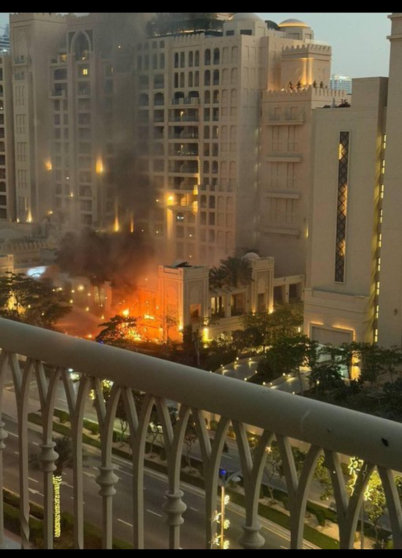
JUST IN: 🇮🇷🇦🇪 Iran strikes renowned Burj Al-Arab hotel in Dubai, UAE.


BREAKING: Ray Dalio avertizează că intrăm în „faza finală” a Marelui Ciclu Dalio spune că istoria se repetă în cicluri de ~100 de ani: imperiile cresc și cad pe fond de datorie, tensiuni interne, rivalități geopolitice, șocuri naturale și salturi tehnologice. Mesajul lui: suntem într-un stadiu târziu, iar ordinea globală post-WWII se erodează. Ce vede el acum: • tensiuni SUA–China în creștere • bulă de datorie și presiune pe monede • polarizare și populism intern • risc de „războaie ale capitalului”, devalorizări și conflicte „fierbinți” Recomandarea lui (pe scurt): • mai puțină expunere pe active de tip datorie • aur ca hedge pentru inflație și haos monetar • diversificare și lecții din istorie Dalio spune că trebuie să ne pregătim pentru o perioadă de „mare dezordine” asemănătoare anilor 1930. Urmărește @cryptoaici pentru interpretări clare ale macro-ului — fără zgomot, fără panică.


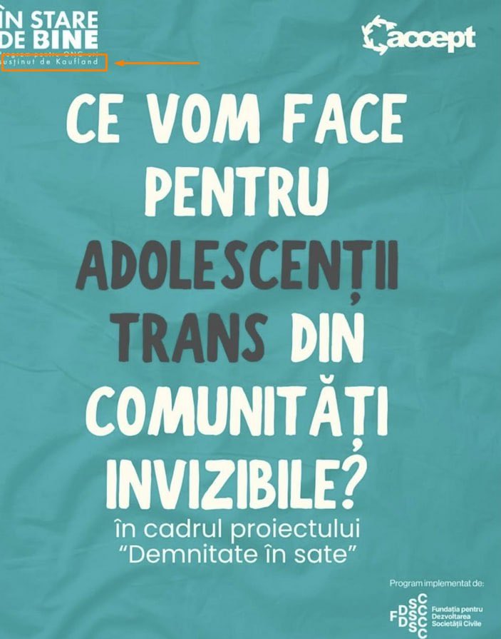
Patria Prima este singurul ONG care lupta contra propagandei LGBTQ. Este incredibil cum au ajuns sa ne urmareasca copiii de la sate, platiti de Kaufland, cu reclama facuta de BRD - Societe Generale prin newsletterul fundatiei lor, Scena9! Unde se va ajunge?