Ravi

633 posts

Ravi

Ravi

@_raviguy

corporate hate tweeting / stream of consciousness / broadcasting my creations into the void

Los Angeles Katılım Temmuz 2014
93 Takip Edilen31 Takipçiler
Ravi
Ravi@_raviguy·
@zackslab @i2cjak Feel free to DM me, I worked through this exact problem with the same micro a few months ago. Would love to help
English
1
0
2
102
zack's lab
zack's lab@zackslab·
okay rough block diagram, what am i missing? feel free to copy @i2cjak:
zack's lab tweet media
zack's lab@zackslab

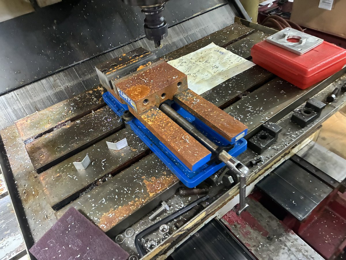
for the @i2cjak 48V dc/dc converter challenge: okay so covering 10mA to 10A current output is going to be more difficult than I thought now that I'm looking at behavior in simulation... approach: - 2 phases, fw will support phase shedding depending on iout. - iout >2A, both phases enabled, CCM - 2A > iout > 500mA, shed 1 phase, CCM - iout < 500mA, 1 phase with some kind of burst/skip scheme still need to figure out how to measure current across the whole range using some combination of sense Rs or DCR of the inductor or some combination.

English
12
1
47
8.1K
Ravi
Ravi@_raviguy·
@Manh_Ti3012 More voltage drop typically means lower noise
English
0
0
1
15
TiManh
TiManh@Manh_Ti3012·
@_raviguy the voltage drop from datasheet is only 0.3V at 1A load. I'm not drawing that much current so will try to lower the voltage gap even more in testing.
English
1
0
1
62
TiManh
TiManh@Manh_Ti3012·
Power supply board for a GaN MMIC. I'm boosting the input voltage to 29 V, then filtering it with two LDOs to get 28 V for each PA stage. It also handles power/bias sequencing. The main PA board is still being worked on.
TiManh tweet media
English
8
4
100
5.1K
Ravi
Ravi@_raviguy·
@willreil It’s technically more of a depaneling machine but it can do the trick if you’re desperate/risk tolerant and it has sharp blades at the right height. The height is killer. Best option may just be clamping straight edges on both sides and hacking away at it with a sharp blade
English
0
0
1
141
Will
Will@willreil·
@_raviguy Maybe I should just buy a v cut machine hahaha
English
3
0
8
1.6K
Will
Will@willreil·
The absolute worst thing possible happened. I ordered the boards with a v-score so I could snap them apart into 9 separate boards, they did not come with it. I don’t even know where to go from here, so incredibly bummed. I guess I will have to order some more boards.
English
129
4
177
26.3K
Ravi
Ravi@_raviguy·
@HiFourPac @willreil It’s definitely iffy cutting without a guide, more suited for depaneling. But in a pinch I’ve used it
English
0
0
1
16
Terry Phillips
Terry Phillips@HiFourPac·
@willreil Technically, those are designed to separate pre v-scored PCBs. Not sure how well that would do at cutting non-scored PCB. Without adding a custom slide table, the first issue would be simply keeping a straight line.
English
2
0
3
449
Will
Will@willreil·
Maybe this is a good time to buy some equipment. How much does one of these things run?
Ravi@_raviguy

@willreil Inquire at your local PCB assembly house to use their V-score cutter

English
18
1
43
7.5K
Ravi
Ravi@_raviguy·
@zackslab Basso has amazing books that will tell you everything you need to know as far as compensation and your boost converter plant model.
English
0
0
0
74
zack's lab
zack's lab@zackslab·
my thoughts so far: > probably going to interleave at least 2 phases > going with an ST part bc i don't want to use TIs toolchain > probably synchronous, although forgoing the diode probably isn't a HUGE efficiency save, will make firmware easier, need to look into this more > installing matlab, reading about controls for the next day or so, going to sim in matlab rather than spice
zack's lab@zackslab

I FORMALLY CHALLENGE THEE (@i2cjak) TO AN EE DESIGN CHALLENGE (rendered in the TONE of an i2cjak wannabEE ARTICLE): ANON… I HAVE A PROPOSAL. a DESIGN CHALLENGE. a TEST of SKILL. a TEST of GRIT. a TEST of whether you are a REAL ELECTRONICS ENGINEER or merely someone who COPY PASTAS application notes written by some TI intern named KYLE. let me set the stage... imagine a world where you need to convert 12v into 48v. this is not a crazy number. this is just BOOSTING a voltage. people have been doing this since before your GREAT GREAT grandparents knew what a transistor was (i2cjack just turned 14). and yet… what does an i2cjak do? he goes to MOUSER (he was banned from digikey) and he types: "BOOST CONVERTER" he grabs some $6.37 switching regulator IC that hardly has any stock, has 87 internal op amps, slope compensation, cmc, undervoltage lockout, soft start, thermal shutdown, brownout detect, a coffee maker, and a SMALL GOBLIN that tunes the loop compensation FOR HIM. he then looks himself in the mirror and calls himself A HARDTECH ENGINEER. he slaps down one inductor, a diode, some caps, and a prayer. NO. not today anon. THE CHALLENGE: • design a 12v to 48v dc/dc converter • highest efficiency @ 10A/480W wins but there are RULES. and they are CRUEL. RULES: • NO SWITCHING REGULATOR ICS • no boost controllers • no flyback controllers • no "smart power stages" • no little black boxes that say "PWM controller" on the datasheet • if the datasheet contains the phrase "switching regulator" you are DISQUALIFIED ALLOWED COMPONENTS: • a microcontroller • gate drivers (maybe) • power transistors • diodes • discrete analog • discrete logic • passives THE CONTROL LOOP: • must be written entirely BY YOU • no OTS analog compensation network that MAGICALLY stabilizes everything YOU WILL: • fab the board at a fab house of your choice • solder it YOURSELF • measure voltages YOURSELF • measure currents YOURSELF • perform step response YOURSELF • perform load sweeps YOURSELF • measure EFFICIENCY YOURSELF • you know, REAL EE SHIT YOURSELF like the founding fvcking fathers intended. ANY TOPOLOGY IS FAIR GAME: • boost • flyback • forward • pushpull • interleaved • some cursed topology you invented at 3am i do not care. but it must convert 12v to 48v. and it must fvck. SCORING: highest measured efficiency @ 10A wins (adjusted for BOM cost). WHY THIS IS FUN: because suddenly all the stuff those nice little regulator ICs do for you becomes YOUR PROBLEM. you must engineer. ELECTRICALLY. things like: • current limiting • duty cycle saturation • loop stability • slope compensation • dead time • gate drive timing • startup behavior • transient response EXPECTED OUTCOMES: • REAL EE is harder than it looks, i might fail. you might fail. BUT WE ALL LEARN. • writing a control loop from scratch is CURSED. • switch node ringing is DEMONIC. and guess what i2cjak, the inductor you'll pick will be WRONG!!! your efficiency will mysteriously drop by 15% because physics HATES YOU!!! but, you are a MANIAC. and you will eventually produce something BEAUTIFUL even IF it is covered in your BLOOD, SWEAT, AND TEARS. so anon. do you ACCEPT the challenge? or will you retreat back to your TPS5430 application notes like a frightened little B*TCH? MAY THE SUPREME WIZARD OF ELECTRONS WIN!!!

English
12
1
28
3.6K
Ravi
Ravi@_raviguy·
@i2cjak @zackslab @AnasYMalas I would argue it’s the perfect amount of integration. Discrete gate drives are a pain and reduction in switch mode area is fantastic
English
0
0
1
12
zack's lab
zack's lab@zackslab·
I FORMALLY CHALLENGE THEE (@i2cjak) TO AN EE DESIGN CHALLENGE (rendered in the TONE of an i2cjak wannabEE ARTICLE): ANON… I HAVE A PROPOSAL. a DESIGN CHALLENGE. a TEST of SKILL. a TEST of GRIT. a TEST of whether you are a REAL ELECTRONICS ENGINEER or merely someone who COPY PASTAS application notes written by some TI intern named KYLE. let me set the stage... imagine a world where you need to convert 12v into 48v. this is not a crazy number. this is just BOOSTING a voltage. people have been doing this since before your GREAT GREAT grandparents knew what a transistor was (i2cjack just turned 14). and yet… what does an i2cjak do? he goes to MOUSER (he was banned from digikey) and he types: "BOOST CONVERTER" he grabs some $6.37 switching regulator IC that hardly has any stock, has 87 internal op amps, slope compensation, cmc, undervoltage lockout, soft start, thermal shutdown, brownout detect, a coffee maker, and a SMALL GOBLIN that tunes the loop compensation FOR HIM. he then looks himself in the mirror and calls himself A HARDTECH ENGINEER. he slaps down one inductor, a diode, some caps, and a prayer. NO. not today anon. THE CHALLENGE: • design a 12v to 48v dc/dc converter • highest efficiency @ 10A/480W wins but there are RULES. and they are CRUEL. RULES: • NO SWITCHING REGULATOR ICS • no boost controllers • no flyback controllers • no "smart power stages" • no little black boxes that say "PWM controller" on the datasheet • if the datasheet contains the phrase "switching regulator" you are DISQUALIFIED ALLOWED COMPONENTS: • a microcontroller • gate drivers (maybe) • power transistors • diodes • discrete analog • discrete logic • passives THE CONTROL LOOP: • must be written entirely BY YOU • no OTS analog compensation network that MAGICALLY stabilizes everything YOU WILL: • fab the board at a fab house of your choice • solder it YOURSELF • measure voltages YOURSELF • measure currents YOURSELF • perform step response YOURSELF • perform load sweeps YOURSELF • measure EFFICIENCY YOURSELF • you know, REAL EE SHIT YOURSELF like the founding fvcking fathers intended. ANY TOPOLOGY IS FAIR GAME: • boost • flyback • forward • pushpull • interleaved • some cursed topology you invented at 3am i do not care. but it must convert 12v to 48v. and it must fvck. SCORING: highest measured efficiency @ 10A wins (adjusted for BOM cost). WHY THIS IS FUN: because suddenly all the stuff those nice little regulator ICs do for you becomes YOUR PROBLEM. you must engineer. ELECTRICALLY. things like: • current limiting • duty cycle saturation • loop stability • slope compensation • dead time • gate drive timing • startup behavior • transient response EXPECTED OUTCOMES: • REAL EE is harder than it looks, i might fail. you might fail. BUT WE ALL LEARN. • writing a control loop from scratch is CURSED. • switch node ringing is DEMONIC. and guess what i2cjak, the inductor you'll pick will be WRONG!!! your efficiency will mysteriously drop by 15% because physics HATES YOU!!! but, you are a MANIAC. and you will eventually produce something BEAUTIFUL even IF it is covered in your BLOOD, SWEAT, AND TEARS. so anon. do you ACCEPT the challenge? or will you retreat back to your TPS5430 application notes like a frightened little B*TCH? MAY THE SUPREME WIZARD OF ELECTRONS WIN!!!
zack's lab tweet media
English
58
22
473
44K
zack's lab
zack's lab@zackslab·
@AnasYMalas @i2cjak i was thinking about GaN but those EPC packages are a bitch to work with. we are hand soldering, going to hedge my bets and not waste time chasing soldering issues. but yes, GaN would win efficiency for sure.
English
6
0
10
10.2K
Anas
Anas@BitsFlareDev·
@zackslab @i2cjak Test efficiency,load sweeps at 48V 10A? How do you do that? The DC electronic loads of that class are pretty expensive.
English
2
0
5
531
Ravi
Ravi@_raviguy·
@yacineMTB Everything is too close to the edges for any mass production
English
0
0
2
689
kache
kache@yacineMTB·
i'm looking for feedback, thank you here's the full definition of my schematic: import { mkdirSync, writeFileSync } from "node:fs" import path from "node:path" import { defineCircuit, definePart, exportKiCadNetlist, instantiate, net, pin, } from "../../../tools/circuitd/src" const ch32v203f8u6 = definePart({ id: "CH32V203F8U6", kicadSymbol: "tinybee:CH32V203F8U6", footprint: "tinybee:QFN-20_L3.0-W3.0-P0.40-BL-EP1.7", defaultValue: "CH32V203F8U6", datasheet: "ch32-riscv-ug.github.io/CH32V20x/datas…", description: "144 MHz RISC-V MCU with ADCs, op-amps, advanced timers, and SWD", fields: { "LCSC Part": "C7570477", }, designNotes: [ "Power this MCU from a 3.3 V rail only; do not allow the VDD pin to see more than 3.6 V.", "Place a 100 nF decoupler immediately next to VDD and the QFN ground return, and keep that loop as short as possible.", "Put a small series resistor between PA0 and any off-board throttle or one-wire configuration signal so the MCU pin is not directly exposed at the connector.", "Keep PA13 and PA14 easy to probe and free of hard loads so SWD still works during bring-up and recovery.", "Keep PA8, PA9, PA10, PA7, PB0, and PB1 on the three phase-drive nets, and keep PA6/BKI free for a future fault or protection input.", "If you follow the openwch RISC-V ESC zero-cross scheme, tie PA3 and PA4 back into PA2 externally and reserve PA2 for that shared interrupt net.", "Route back-EMF and op-amp related pins away from phase copper, gate-drive loops, and other fast-switching nodes.", ], pins: { "PA0/WKUP/ADC0": "1", "PA1/ADC1": "2", "PA2/ADC2/OP2O0": "3", "PA3/ADC3/OP1O0": "4", "PA4/ADC4/OP2O1": "5", "PA5/ADC5/OP2N1": "6", "PA7/ADC7/OP2P1/CH1N": "7", "PB0/ADC8/OP1P1/CH2N": "8", "PB1/ADC9/OP1O1/CH3N": "9", "PB10/OP2N0": "10", "PB11/OP1N0": "11", "PB14/OP2P0": "12", "PB15/OP1P0": "13", "PA8/CH1": "14", "PA9/CH2": "15", "PA13/SWD/PA12/UDP": "16", "PA14/SWC/PA11/UDM": "17", "PA10/CH3": "18", VDD: "19", "PA6/ADC6/OP1N1/BKI": "20", GND: "21", }, }) const tlv75533pdqnt = definePart({ id: "TLV75533PDQNT", kicadSymbol: "Regulator_Linear:TLV75533PDBV", footprint: "tinybee:Texas_X2SON-4_1x1mm_P0.65mm", defaultValue: "TLV75533PDQNT", datasheet: "ti.com/lit/ds/symlink…", description: "500mA low-dropout fixed 3.3V regulator in 1x1mm X2SON-4", designNotes: [ "Treat +BATT as a 1S Li-ion or LiPo rail only; this regulator has a 5.5 V maximum input rating, so 2S or higher is out of bounds for this graph.", "Place at least 1 uF ceramic directly at IN and at least 1 uF ceramic directly at OUT; do not push those capacitors away from the package.", "Check regulator heating with (VIN - 3.3 V) * load current and add copper area if the dissipation is not comfortably safe.", "Add local input bulk when the battery lead is long or inductive so the LDO input does not absorb line spikes by itself.", "Keep EN tied to a known state at all times; if startup control matters later, break it out deliberately instead of bodging it in.", "The X2SON thermal pad is internally tied to GND; flood it into the local ground copper and do not leave the center pad floating.", ], pins: { OUT: "1", GND: "2", EN: "3", IN: "4", THERMAL_PAD: "5", }, }) const controlHeader = definePart({ id: "CTRL_IN_HEADER_1X01", kicadSymbol: "Connector_Generic:Conn_01x01", footprint: "tinybee:CTRL_PAD_1x01_Micro", defaultValue: "CTRL_IN", description: "1-pin control input wire pad for throttle signal", designNotes: [ "Use this only for the control signal.", "Ground reference is expected to be shared elsewhere in the system when this pad is in use.", "Battery power comes in through the dedicated battery wire holes, not through this control pad.", "PA0 on the CH32 is not a true FT input; treat this header as a 3.3 V logic input unless you deliberately add a real level-conditioning stage.", ], pins: { PIN1: "1", }, }) const motorHeader = definePart({ id: "MOTOR_OUT_HEADER_1X03", kicadSymbol: "Connector_Generic:Conn_01x03", footprint: "tinybee:MOTOR_PADS_1x03_Micro", defaultValue: "MOTOR_OUT", description: "3-pin motor phase wire pad group", designNotes: [ "This is the board edge interface for the three motor phases.", "Use direct wire holes here rather than a bulky 2.54 mm header footprint.", ], pins: { PIN1: "1", PIN2: "2", PIN3: "3", }, }) const programmingHeader = definePart({ id: "PROG_HEADER_1X04", kicadSymbol: "Connector_Generic:Conn_01x04", footprint: "tinybee:PROG_PADS_1x04_Micro", defaultValue: "PROG", description: "4-pin fine-pitch SWD programming header", designNotes: [ "Break out SWDIO, SWCLK, GND, and 3.3 V so the CH32 can be flashed and recovered without bodge wires.", "Keep this header free of extra loading and avoid reusing the SWD pins elsewhere until firmware bring-up is stable.", "Treat the 3.3 V pin here as target reference unless you deliberately design reverse-current-safe back-powering through the regulator path.", ], pins: { PIN1: "1", PIN2: "2", PIN3: "3", PIN4: "4", }, }) const batteryHeader = definePart({ id: "BATT_IN_HEADER_1X02", kicadSymbol: "Connector_Generic:Conn_01x02", footprint: "tinybee:BATT_PADS_1x02_Micro", defaultValue: "BATT_IN", description: "2-pin battery wire pad pair", designNotes: [ "Use this dedicated pair for battery positive and battery negative input.", "Keep the battery loop tight to the bulk capacitors and half-bridge supply entry.", ], pins: { PIN1: "1", PIN2: "2", }, }) const complementaryHalfBridge = definePart({ id: "PMCPB5530X_115", kicadSymbol: "tinybee:PMCPB5530X,115", footprint: "tinybee:DFN2020-6_L2.0-W2.0-P0.65-BL", defaultValue: "PMCPB5530X,115", datasheet: "assets.nexperia.com/documents/data…", description: "20 V complementary N/P MOSFET half-bridge in DFN2020-6", fields: { "LCSC Part": "C552747", }, designNotes: [ "Use this complementary half-bridge only on a 1S Li-ion or LiPo rail; do not reuse the direct P-gate pull-down topology above the 1S battery range.", "With +BATT limited to the 1S range, the direct P-gate pull-down swing stays inside the device gate limits and gives usable drive headroom.", "Drive the low-side N-FET gates directly from the 3.3 V timer outputs only in this 1S design; rework the stage before raising the battery voltage.", "Do not skimp on local +BATT bypass; keep real ceramic bulk plus a high-frequency bypass capacitor tight to the half-bridge supply loop.", "Pour the duplicated drain pads into real copper for current and heat spreading; do not neck them down right at the package.", "Keep each gate loop short, tight, and referenced to its own source return to reduce ringing and false turn-on.", "Assume the board copper sets the real current limit; check temperature rise on the actual ESC geometry, not only the datasheet headline current.", ], pins: { LOW_SIDE_SOURCE: "1", LOW_SIDE_GATE: "2", HIGH_SIDE_DRAIN: ["3", "8"], HIGH_SIDE_SOURCE: "4", HIGH_SIDE_GATE: "5", LOW_SIDE_DRAIN: ["6", "7"], }, }) const highSidePullDownBjt = definePart({ id: "BC847BLP_7", kicadSymbol: "Transistor_BJT:Q_NPN_BEC", footprint: "Package_TO_SOT_SMD:SOT-883", defaultValue: "BC847BLP-7", datasheet: "wmsc.lcsc.com/wmsc/upload/fi…", description: "45 V, 100 mA NPN small-signal transistor in SOT-883", designNotes: [ "Use this device only as the helper pull-down for the high-side P-gate nets; do not put motor or supply current through it as a power path element.", "In this topology, keep emitter at GND, collector on the P-gate net, and drive the base through a resistor from the MCU.", "Give the base a defined pulldown so the PMOS high side stays off while the MCU is in reset or high-impedance.", "With a 470R P-gate pull-up on a 1S rail, this transistor sinks about 9 mA at full turn-on, which is still well inside the BC847BLP-7's capability.", "Check the B-E-C pin order against the footprint before layout release; small BJTs are easy to rotate or mirror by accident.", ], pins: { BASE: "1", EMITTER: "2", COLLECTOR: "3", }, }) const yageoRc0201Datasheet = "mouser.com/datasheet/2/44…" const kemetMlccDatasheet = "content.kemet.com/datasheets/CER…" const defineYageoRc0201 = (mpn: string, value: string) => definePart({ id: mpn, kicadSymbol: "Device:R", footprint: "Resistor_SMD:R_0201_0603Metric", defaultValue: value, datasheet: yageoRc0201Datasheet, description: `Yageo ${mpn} 0201 1% thick-film resistor`, fields: { Manufacturer: "Yageo", MPN: mpn, Tolerance: "1%", Power: "0.05W", }, designNotes: [ "This BOM is locked to an exact Yageo RC0201FR-07 1% resistor, not a generic 0201 placeholder.", "Keep the 1% series on the back-EMF divider path so thresholds stay predictable across temperature.", "Re-check pulse and dissipation stress if the battery domain or gate network changes.", ], pins: { A: "1", B: "2", }, }) const defineYageoRc0402 = (mpn: string, value: string) => definePart({ id: mpn, kicadSymbol: "Device:R", footprint: "Resistor_SMD:R_0402_1005Metric", defaultValue: value, datasheet: "mouser.com/datasheet/2/44…", description: `Yageo ${mpn} 0402 1% thick-film resistor`, fields: { Manufacturer: "Yageo", MPN: mpn, Tolerance: "1%", Power: "0.063W", }, designNotes: [ "Use 0402 here where the resistor sees non-trivial continuous dissipation on the switching rail.", "Do not silently shrink these positions back to 0201 without re-checking power and temperature margin.", ], pins: { A: "1", B: "2", }, }) const defineKemetMlcc = ({ mpn, value, footprint, description, voltage, dielectric, designNotes, }: { mpn: string value: string footprint: string description: string voltage: string dielectric: string designNotes: readonly string[] }) => definePart({ id: mpn, kicadSymbol: "Device:C", footprint, defaultValue: value, datasheet: kemetMlccDatasheet, description, fields: { Manufacturer: "KEMET", MPN: mpn, Dielectric: dielectric, "Rated Voltage": voltage, }, designNotes, pins: { POS: "1", NEG: "2", }, }) const resistor30r = defineYageoRc0201("RC0201FR-0730RL", "30R") const resistor470r0402 = defineYageoRc0402("RC0402FR-07470RL", "470R") const resistor1k = defineYageoRc0201("RC0201FR-071KL", "1k") const resistor10k = defineYageoRc0201("RC0201FR-0710KL", "10k") const resistor100k = defineYageoRc0201("RC0201FR-07100KL", "100k") const resistor12k = defineYageoRc0201("RC0201FR-0712KL", "12k") const resistor15k = defineYageoRc0201("RC0201FR-0715KL", "15k") const resistor33k = defineYageoRc0201("RC0201FR-0733KL", "33k") const swdVrefIsolationDiode = definePart({ id: "RB751CS40,315", kicadSymbol: "Device:D_Schottky", footprint: "tinybee:D_SOD-882", defaultValue: "RB751CS40,315", datasheet: "nexperia.com/product/RB751C…", description: "40 V small-signal Schottky diode in SOD-882 for isolated SWD Vref sensing", designNotes: [ "This diode lets the programming header sense the target 3.3 V rail without back-powering the TLV755 when an external tool drives Vref.", "Place it close to the programming pads, and keep the +3V3 cathode side on the board rail with the isolated anode side only on the header Vref pin.", ], pins: { K: "1", A: "2", }, }) const capacitor100nF0402 = defineKemetMlcc({ mpn: "C0402C104K4RACTU", value: "100nF", footprint: "Capacitor_SMD:C_0402_1005Metric", description: "KEMET 100nF 16V X7R MLCC, 0402", voltage: "16V", dielectric: "X7R", designNotes: [ "This exact 16 V X7R part is locked for the 100 nF bypass positions in this 1S design.", "Use it for local high-frequency bypass on +BATT or V3.3; do not silently substitute a lower-voltage or poor-stability dielectric.", ], }) const capacitor100nF0201 = defineKemetMlcc({ mpn: "C0201C104K9PACTU", value: "100nF", footprint: "Capacitor_SMD:C_0201_0603Metric", description: "KEMET 100nF 6.3V X5R MLCC, 0201", voltage: "6.3V", dielectric: "X5R", designNotes: [ "Use this only for local low-voltage decoupling like the CH32 VDD bypass.", "Do not silently reuse this 0201 part on the battery rail; keep the battery-facing 100 nF positions on the 16 V 0402 part.", ], }) const capacitor1uF0402 = defineKemetMlcc({ mpn: "C0402C105K8PAC7411", value: "1uF", footprint: "Capacitor_SMD:C_0402_1005Metric", description: "KEMET 1uF 10V X5R MLCC, 0402", voltage: "10V", dielectric: "X5R", designNotes: [ "This exact 10 V X5R part is the TLV755 output capacitor and satisfies the regulator's 1 uF ceramic requirement.", "A 0402 body is acceptable here, but this is still a regulator output part, not a battery-domain bypass; do not shrink it further without checking bias derating and stability.", ], }) const capacitor22uF0805 = defineKemetMlcc({ mpn: "C0805C226M8PACTU", value: "22uF", footprint: "Capacitor_SMD:C_0805_2012Metric", description: "KEMET 22uF 10V X5R MLCC, 0805", voltage: "10V", dielectric: "X5R", designNotes: [ "This exact 10 V X5R 0805 part is the 1S battery-side bulk capacitor.", "Keep this input bulk capacitor in 0805 or larger; do not shrink it back to 0603 without re-checking effective capacitance at 1S bias.", ], }) const C1 = instantiate(capacitor1uF0402, "C1") const C2 = instantiate(capacitor100nF0201, "C2") const C3 = instantiate(capacitor100nF0402, "C3") const C4 = instantiate(capacitor22uF0805, "C4") const C5 = instantiate(capacitor100nF0201, "C5") const C6 = instantiate(capacitor22uF0805, "C6") const Q1 = instantiate(complementaryHalfBridge, "Q1") const Q2 = instantiate(complementaryHalfBridge, "Q2") const Q3 = instantiate(complementaryHalfBridge, "Q3") const Q4 = instantiate(highSidePullDownBjt, "Q4") const Q5 = instantiate(highSidePullDownBjt, "Q5") const Q6 = instantiate(highSidePullDownBjt, "Q6") const J_CTRL = instantiate(controlHeader, "J_CTRL") const J_BATT = instantiate(batteryHeader, "J_BATT") const J_MOTOR = instantiate(motorHeader, "J_MOTOR") const TP_PROG = instantiate(programmingHeader, "TP_PROG") const D1 = instantiate(swdVrefIsolationDiode, "D1") const R1 = instantiate(resistor30r, "R1") const R2 = instantiate(resistor1k, "R2") const R3 = instantiate(resistor10k, "R3") const R4 = instantiate(resistor470r0402, "R4") const R5 = instantiate(resistor30r, "R5") const R6 = instantiate(resistor1k, "R6") const R7 = instantiate(resistor10k, "R7") const R8 = instantiate(resistor470r0402, "R8") const R9 = instantiate(resistor30r, "R9") const R10 = instantiate(resistor1k, "R10") const R11 = instantiate(resistor10k, "R11") const R12 = instantiate(resistor470r0402, "R12") const R13 = instantiate(resistor15k, "R13") const R14 = instantiate(resistor33k, "R14") const R15 = instantiate(resistor100k, "R15") const R16 = instantiate(resistor15k, "R16") const R17 = instantiate(resistor33k, "R17") const R18 = instantiate(resistor100k, "R18") const R19 = instantiate(resistor15k, "R19") const R20 = instantiate(resistor33k, "R20") const R21 = instantiate(resistor100k, "R21") const R22 = instantiate(resistor100k, "R22") const R23 = instantiate(resistor100k, "R23") const R24 = instantiate(resistor100k, "R24") const R25 = instantiate(resistor12k, "R25") const R26 = instantiate(resistor33k, "R26") const R27 = instantiate(resistor1k, "R27") const U1 = instantiate(tlv75533pdqnt, "U1") const U2 = instantiate(ch32v203f8u6, "U2") const tinybeeEscChannel = defineCircuit({ name: "tinybee-esc-channel", source: "projects/tinybee/circuitd/tinybee-esc-channel.ts", description: "1S CH32-based tinybee ESC channel aligned to the openwch RISC-V_ESC V203 pinout", parts: [ C1, C2, C3, C4, C5, C6, D1, J_BATT, J_CTRL, J_MOTOR, Q1, Q2, Q3, Q4, Q5, Q6, R1, R2, R3, R4, R5, R6, R7, R8, R9, R10, R11, R12, R13, R14, R15, R16, R17, R18, R19, R20, R21, R22, R23, R24, R25, R26, R27, TP_PROG, U1, U2, ], nets: [ net( "+BATTERY", pin(J_BATT, "PIN1"), pin(C3, "POS"), pin(C4, "POS"), pin(C6, "POS"), pin(Q1, "HIGH_SIDE_SOURCE"), pin(Q2, "HIGH_SIDE_SOURCE"), pin(Q3, "HIGH_SIDE_SOURCE"), pin(R4, "B"), pin(R8, "B"), pin(R12, "B"), pin(R25, "B"), pin(U1, "IN"), pin(U1, "EN"), ), net("/ADC_VOLTAGE_SENSE", pin(C5, "POS"), pin(R25, "A"), pin(R26, "B"), pin(U2, "PA1/ADC1")), net("/A_HIGH_COMMAND", pin(R2, "B"), pin(U2, "PA10/CH3")), net("/A_LOW_COMMAND", pin(R1, "B"), pin(U2, "PB1/ADC9/OP1O1/CH3N")), net("/A_HIGH_CONTROL", pin(Q4, "BASE"), pin(R2, "A"), pin(R3, "B")), net("/A_LOW_GATE", pin(Q1, "LOW_SIDE_GATE"), pin(R1, "A"), pin(R22, "B")), net("/A_P_GATE", pin(Q1, "HIGH_SIDE_GATE"), pin(Q4, "COLLECTOR"), pin(R4, "A")), net("/A_BACK_EMF", pin(R13, "A"), pin(R14, "B"), pin(R15, "A"), pin(U2, "PA5/ADC5/OP2N1")), net("/B_BACK_EMF", pin(R16, "A"), pin(R17, "B"), pin(R18, "A"), pin(U2, "PB10/OP2N0")), net("/C_BACK_EMF", pin(R19, "A"), pin(R20, "B"), pin(R21, "A"), pin(U2, "PB11/OP1N0")), net("/BACK_EMF_COMMON", pin(R15, "B"), pin(R18, "B"), pin(R21, "B"), pin(U2, "PB14/OP2P0"), pin(U2, "PB15/OP1P0")), net("/B_HIGH_COMMAND", pin(R6, "B"), pin(U2, "PA9/CH2")), net("/B_LOW_COMMAND", pin(R5, "B"), pin(U2, "PB0/ADC8/OP1P1/CH2N")), net("/B_HIGH_CONTROL", pin(Q5, "BASE"), pin(R6, "A"), pin(R7, "B")), net("/B_LOW_GATE", pin(Q3, "LOW_SIDE_GATE"), pin(R5, "A"), pin(R23, "B")), net("/B_P_GATE", pin(Q3, "HIGH_SIDE_GATE"), pin(Q5, "COLLECTOR"), pin(R8, "A")), net("/C_HIGH_COMMAND", pin(R10, "B"), pin(U2, "PA8/CH1")), net("/C_LOW_COMMAND", pin(R9, "B"), pin(U2, "PA7/ADC7/OP2P1/CH1N")), net("/C_HIGH_CONTROL", pin(Q6, "BASE"), pin(R10, "A"), pin(R11, "B")), net("/C_LOW_GATE", pin(Q2, "LOW_SIDE_GATE"), pin(R9, "A"), pin(R24, "B")), net("/C_P_GATE", pin(Q2, "HIGH_SIDE_GATE"), pin(Q6, "COLLECTOR"), pin(R12, "A")), net("/PWM_INPUT", pin(J_CTRL, "PIN1"), pin(R27, "A")), net("/PWM_INPUT_MCU", pin(R27, "B"), pin(U2, "PA0/WKUP/ADC0")), net("/OPA_ZERO_CROSS_INTERRUPT", pin(U2, "PA2/ADC2/OP2O0"), pin(U2, "PA3/ADC3/OP1O0"), pin(U2, "PA4/ADC4/OP2O1")), net("/PHASE_A", pin(J_MOTOR, "PIN1"), pin(Q1, "HIGH_SIDE_DRAIN"), pin(Q1, "LOW_SIDE_DRAIN"), pin(R13, "B")), net("/PHASE_B", pin(J_MOTOR, "PIN2"), pin(Q3, "HIGH_SIDE_DRAIN"), pin(Q3, "LOW_SIDE_DRAIN"), pin(R16, "B")), net("/PHASE_C", pin(J_MOTOR, "PIN3"), pin(Q2, "HIGH_SIDE_DRAIN"), pin(Q2, "LOW_SIDE_DRAIN"), pin(R19, "B")), net("/SWD_CLOCK", pin(TP_PROG, "PIN1"), pin(U2, "PA14/SWC/PA11/UDM")), net("/SWD_DATA", pin(TP_PROG, "PIN2"), pin(U2, "PA13/SWD/PA12/UDP")), net("/SWD_VREF", pin(D1, "A"), pin(TP_PROG, "PIN4")), net( "GND", pin(J_BATT, "PIN2"), pin(C1, "NEG"), pin(C2, "NEG"), pin(C3, "NEG"), pin(C4, "NEG"), pin(C6, "NEG"), pin(Q1, "LOW_SIDE_SOURCE"), pin(Q2, "LOW_SIDE_SOURCE"), pin(Q3, "LOW_SIDE_SOURCE"), pin(Q4, "EMITTER"), pin(Q5, "EMITTER"), pin(Q6, "EMITTER"), pin(R3, "A"), pin(R7, "A"), pin(R11, "A"), pin(R14, "A"), pin(R17, "A"), pin(R20, "A"), pin(R22, "A"), pin(R23, "A"), pin(R24, "A"), pin(R26, "A"), pin(C5, "NEG"), pin(TP_PROG, "PIN3"), pin(U1, "GND"), pin(U1, "THERMAL_PAD"), pin(U2, "GND"), ), net("+3V3", pin(C1, "POS"), pin(C2, "POS"), pin(D1, "K"), pin(U1, "OUT"), pin(U2, "VDD")), net("unconnected-(U2-PA6{slash}ADC6{slash}OP1N1{slash}BKI-Pad20)", pin(U2, "PA6/ADC6/OP1N1/BKI")), ], }) const outputPath = path.resolve(__dirname, "generated", "tinybee-esc-channel.net") const main = () => { mkdirSync(path.dirname(outputPath), { recursive: true }) writeFileSync(outputPath, exportKiCadNetlist(tinybeeEscChannel), "utf8") process.stdout.write(`${outputPath}\n`) } if (import.meta.main) { main() } export { tinybeeEscChannel } export default tinybeeEscChannel
English
36
4
279
25K
free_as_a_bird
free_as_a_bird@Stefan_btw·
@HowThingsWork_ Can someone explain me in a proper way what he has done here? After cleaning the brazing points…what kind of liquid did he use
English
3
0
5
5.8K
HOW THINGS WORK
HOW THINGS WORK@HowThingsWork_·
Precision required here with this repair 🤏🏼
English
160
733
17.1K
3.4M
Kaleb Reinhart
Kaleb Reinhart@t3nable·
@serteceg Yeah I will have to just spend a little time with it. Sprayed the shit out of it with WD40 and will let it soak overnight.
English
3
0
3
882
Kaleb Reinhart
Kaleb Reinhart@t3nable·
Oh my god it’s so sad. I had the overhead door open for a bit last weekend when it was humid af and just noticed the mill 😞
Kaleb Reinhart tweet mediaKaleb Reinhart tweet media
English
39
2
235
26.9K
Ravi
Ravi@_raviguy·
@yacineMTB Yes 0201 is for the best engineers only it will allow you to quickly join their ranks. Make sure you use the largest capacitors available in 0201 for maximum value
English
1
0
9
1.3K
kache
kache@yacineMTB·
why shouldn't i just pick the smallest possible cap/resistor sizes if i'm going to get it assembled by a board shop? is there any reason other than being a stinky incapable human to get bigger sizes than 201
English
61
2
125
21.7K
Ravi
Ravi@_raviguy·
@beezkneez6969 @mSanterre Besides the careless placement, it’s that all these projects are always the most basic beginner blink projects. Never anything impressive
English
0
0
1
7
max
max@mSanterre·
It's over for EEs, AI can generate perfect PCBs.
max tweet media
English
7
0
14
9.5K