Sabitlenmiş Tweet
人虽不强有弓一长
2K posts

人虽不强有弓一长
@guoqiang
产业分析师和技术分析师,璞玉智库和阅码场创始人。正在成为一个准博物学家的路上。
Beijing Katılım Ocak 2009
1K Takip Edilen668 Takipçiler
先进封装发力。
Dan Nystedt@dnystedt
Intel has placed big orders for advanced packaging production line equipment to firms in Taiwan, media report, citing unnamed supply chain sources, and adding the equipment is for capacity expansion in Intel plants in Oregon and Vietnam. Taiwan equipment suppliers include E&R Engineering, C Sun Manufacturing, Ableprint Technology. $INTC #semiconductors #EMIB investor.com.tw/onlinenews/New…
中文
人虽不强有弓一长 retweetledi

We now have more details about the alleged OpenAI smartphone 🚨
- Mass production could begin in early 2027
- MediaTek expected as the sole chip supplier
- Custom chip based on Dimensity 9600
- Built on TSMC’s advanced N2P node
- LPDDR6 + UFS 5.0
- Major focus on camera/visual AI (ISP) with improved HDR
- Dual-NPU setup for stronger AI performance
- pKVM + inline hashing for enhanced security
Estimated shipments: ~30M units (2027–2028)
Via: .@mingchikuo
(Image for reference)

English

Intel 18A 14A要来了。
当Apple都在台积电产能受困时,AMD更加会无法拿到足够的产能生产足够的供应。这也是我为何看空AMD的原因。
比起产能无法控制的AMD,具有foundry的Intel的竞争力强多了。Intel的重资产模式正在因为地缘政治和逆全球化而变得越来越重要。
控制和具备自身完整的制造体系是非常必要的,这点马斯克做得非常出色。而国家层面上,中国是这方面的霸主。美国在川普主导下也在回归这条必须的路线。
*Walter Bloomberg@DeItaone
$AAPL - APPLE CEO TIM COOK SAYS IPHONE FACED SUPPLY CONSTRAINTS OF ADVANCED NODE CHIPS: REUTERS INTERVIEW
中文
cpu卖爆,ifs绑定头部,布局量子。典型吃着碗里的,看着锅里的,盯着案板上。
PsiQuantum@PsiQuantum
We are thrilled to announce that @LipBuTan1, Intel CEO and longtime veteran of the semiconductor industry, has joined PsiQuantum's Board of Directors. His appointment reflects PsiQuantum's ongoing work to leverage existing semiconductor manufacturing as the company rapidly scales its silicon photonics platform and drives toward deploying utility-scale quantum computers. Learn more: psiquantum.com/news-import/li…
中文
好像中国一重在好多地方都超过JSW了吧。
World Data Analysis@World_Data_A
The steel heart of nuclear power: No Japan no nuclear reactor core Nuclear reactors are often defined by design, capacity, or location. But their most critical component is rarely discussed: the reactor pressure vessel (RPV). At the core of this system are ultra-large steel forgings, massive, single-piece components that must withstand: Extreme heat (up to ~350°C) High pressure (15+ MPa) Decades of radiation exposure If this component fails, the entire plant fails. There is no redundancy. The product These forgings form the “steel heart” of nuclear reactors. They are produced from 600–670 ton steel ingots, shaped under presses up to 14,000 tons, and can reach 10–12 meters in size. Who makes them A very small number of companies globally have this capability. Among them, Japan Steel Works (JSW) stands out. Founded in 1907 Muroran (Hokkaido) is its main facility Decades of experience in nuclear-grade forgings Supplies major reactor projects in Europe, the U.S., China, and Japan Market position JSW has historically claimed around 80% of the global market for large forged components used in nuclear reactors. This does not mean Japan dominates all nuclear construction, but it highlights a critical bottleneck in the supply chain. Where these components are used JSW’s forgings have been used in major reactor designs worldwide: EPR (France) AP1000 (USA) VVER (Finland/China) In many cases, the internal structural core of these reactors originates from Japan. Why this matters This is not a typical manufacturing advantage. Only 5–6 companies globally can produce these components Requires decades of metallurgical expertise Extremely high capital investment Long production cycles (often 2–3 years per unit) This creates a structural chokepoint in the global nuclear supply chain. Regulations and barriers to entry Entry is not just about technology: Must comply with strict nuclear standards (e.g., ASME Section III) Requires approval from multiple regulators (NRC, ASN, etc.) Hundreds of inspections and material tests Once qualified, suppliers are rarely replaced Requalification is so difficult that existing suppliers maintain long-term dominance So these make JSW dominant Source: @WorldNuclear, @AAF, Coral Capital
中文
除了没有晶圆厂来保证产能,其他都对。
Leonard@Leoskie_L
AMD 4月24日衝到歷史新高 $351,目前還在 $326.8 震。 靠北,沒想到還是太低估了。 這不是AMD打敗NVIDIA,是Intel自己拉胯把CPU市場拱手讓人。 18A搞到現在還在掙扎,AMD的ZEN5已經在資料中心殺到35-40%市佔,Meta跟OpenAI更直接砸6GW定制MI450訂單下來。 結果呢?UBS那個Timothy Arcuri昨天直接把目標價從310拉到455! 笑死,連國際大投行都開始承認「還是低估了」 股癌公開持股AMD,現在看起來根本不是買一檔,是買一張「Intel送分題+定制AI大禮包」的雙重保證書。 這不是勝利者的故事,這是「別人倒楣我發財」的經典劇本。 ATH之後還有沒有第三幕? 有,而且劇本已經開始翻頁了,UBS直接把下一頁價格標到$455。 完整文章在這: x.com/Leoskie_L/stat…
中文
人虽不强有弓一长 retweetledi

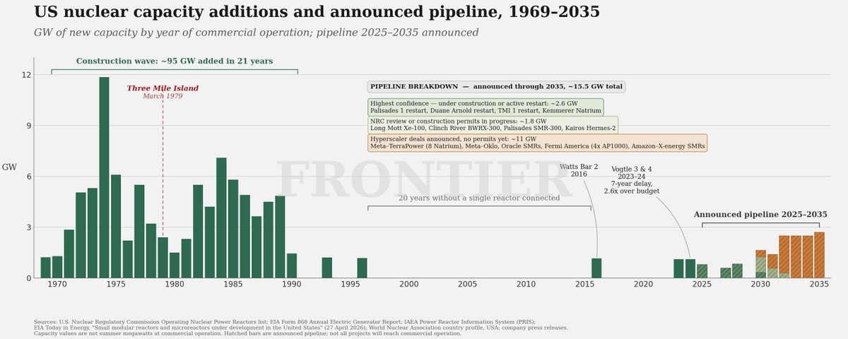
The US nuclear pipeline is resurging after nearly three decades of near-standstill. The country added ~95 GW between 1969 and 1990, then almost nothing until Watts Bar 2 in 2016 and Vogtle 3-4 in 2023-24.
The pipeline announced through 2035 reaches 16 GW: 2.6 GW under construction or active restart (Palisades 1, Duane Arnold, TMI 1, Kemmerer Natrium), while the rest are hyperscaler deals from Meta-TerraPower, Oracle, Fermi America, and Amazon-X-energy, still without NRC permits. EIA tracker: eia.gov/todayinenergy/…
English
人虽不强有弓一长 retweetledi

If those predictions materialise, I have some of mine:
1. HBM demand will probably also accelerate due to the EMIB support for more interfaces than CoWoS.
2. HBM demand will accelerate even further due to the higher number of GPUs being shipped, as currently packaging was a bottleneck.
English
难道今天涨是因为它?
SemiVision👁️👁️@semivision_tw
According to an exclusive report from Taiwan’s DigiTimes, NVIDIA is reportedly planning to shift part of the foundry orders for its next-generation Feynman GPU to Intel. While the critical GPU core is still expected to be manufactured by TSMC, the I/O chiplet responsible for communication is likely to adopt Intel’s 18A or 14A process. Around 25% of the GPUs may also use Intel’s EMIB advanced packaging technology. According to DigiTimes, following NVIDIA’s investment in Intel, the company has preliminarily decided to adopt a dual-foundry model for its “Feynman” architecture platform, scheduled for launch in 2028. This move is seen as a strategic retreat aimed at aligning with “Made in America” policy pressure amid tariff threats from the Trump administration. Current rumors suggest that the Feynman GPU core will remain with TSMC, while the communication I/O die may shift to Intel’s 18A or 14A process. In addition, 25% of the GPUs are expected to use Intel’s EMIB advanced packaging technology. DigiTimes noted that Intel taking part of NVIDIA’s orders could be “more beneficial than harmful” for TSMC. First, modestly giving up some market share could ease regulatory concerns over TSMC’s perceived monopoly. Second, it could help relieve political pressure from the U.S. government. Finally, because the orders flowing to Intel are likely to be smaller-volume and lower-end in nature, TSMC would still retain control over the most advanced and highest-margin core manufacturing processes. This kind of multi-sourcing model is likely to become standard practice for U.S. chipmakers over the next several years. For Intel, the key question will be whether it can deliver competitive 14A yield on schedule by 2028. $INTC open.substack.com/pub/tspasemico…
中文
人虽不强有弓一长 retweetledi

