
Christo Robin
2.9K posts


삼성, 8나노 M램 첫 개발…‘꿈의 메모리’ 주도권 선점
1/
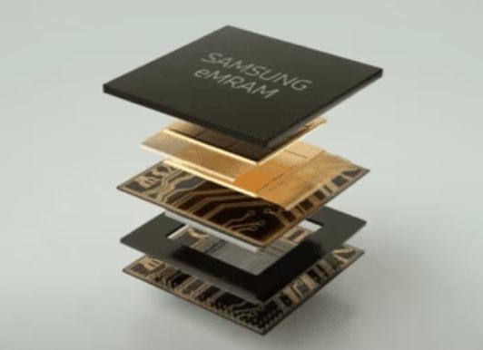
삼성전자가 차세대 메모리인 자기저항메모리 M램에서 업계 최고 수준의 기술을 확보했다.
2/
삼성전자 파운드리사업부 연구진이 국제고체회로학회 ISSCC 2026에서 8나노 핀펫 공정을 적용한 내장형 M램 구현에 성공하고 양산 수율까지 달성했다.
3/
이번 8나노 M램은 기존 14나노 대비 쓰기 속도가 62.5퍼센트 빨라졌고 집적도는 11.5퍼센트 높아졌으며 종합 성능 점수는 52.9퍼센트 개선됐다.
4/
M램은 전원 없이도 데이터를 유지할 수 있고 동작 속도가 낸드플래시보다 1000배 빠르며 D램 수준의 성능을 내는 꿈의 메모리로 불린다.
5/
삼성전자는 2018년 28나노 M램 양산을 시작으로 2024년 14나노, 올해 8나노를 목표로 개발을 진행해왔다.
6/
이번 성공으로 내년 5나노 M램 양산 계획을 차질 없이 추진할 수 있게 됐으며 대만 TSMC와의 경쟁에서도 앞서게 됐다.
7/
AI 반도체와 미래차 분야에서 전력 효율과 성능을 동시에 높일 수 있는 M램이 게임체인저로 부상하면서 삼성전자의 메모리 주도권 강화가 기대된다.
한국어
@King_James_Kim I hope things go right when it goes to Taylor
English


@Alisvolatprop12 Isn't it difficult to reflect same yield in new site
English

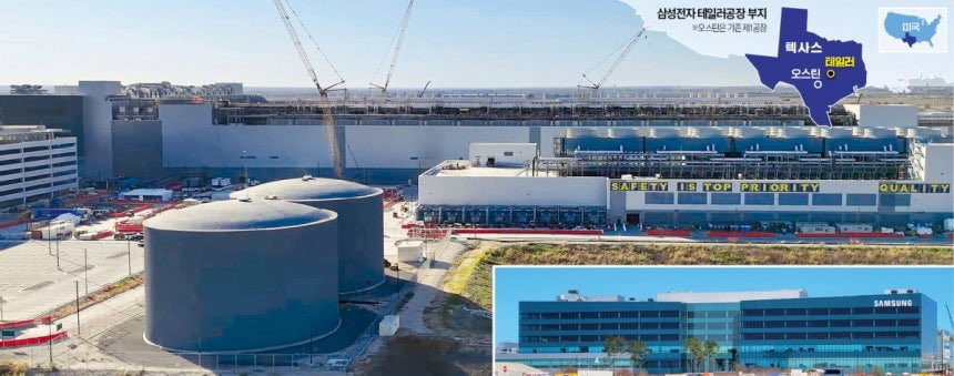
[단독] 삼성 美테일러팹 가동 준비 마쳐…"하반기부터 테슬라칩 양산"
흥미롭군요... 이제 테일러팹과 평택팹간의 수율 차이가 날 지 귀추가 주목됩니다.
hankyung.com/article/202604…
한국어
@blazingbees Also copying this same yield to Taylor is a big challenge
English

@wordingwalking As if HBM it is pretty sure companies will come to samsung. But what i want to see is these companies using samsung foundry
English

"HBM 시장의 또 다른 축인 SK하이닉스와는 별도 면담 없이 삼성전자와의 논의에 집중한 것으로 알려졌다."
거봐 🤭
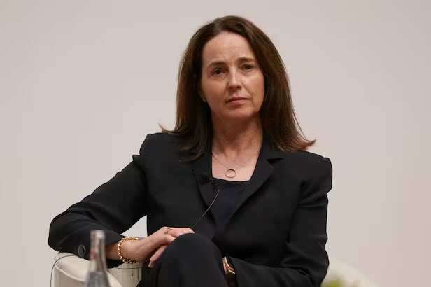
[단독] 오픈AI CFO, 삼성전자와 ‘HBM4’ 공급망 논의… ‘AI 메모리 주도권’ 재편 신호 (출처 : 네이버 뉴스) naver.me/5vJO37yS
한국어
오픈AI CFO, 삼성전자와 HBM4 공급망 논의… AI 메모리 주도권 재편 신호
1/
오픈AI가 고대역폭메모리 HBM4 공급망을 구축하기 위해 삼성전자와 본격 협력 논의를 진행했다.
2/
지난 3월 사라 프라이어 오픈AI 최고재무책임자가 방한해 삼성전자 경영진과 비공개 회담을 가졌다.
3/
회담에서는 HBM4의 공급 물량, 양산 시점, 공급 안정성, 중장기 협력 구조를 집중적으로 논의한 것으로 알려졌다.
4/
오픈AI는 자체 개발 중인 AI 칩 타이탄에 삼성전자의 HBM4를 탑재하는 방안을 구체화하고 있다.
5/
이번 협력은 엔비디아 의존도를 낮추고 메모리 공급 부족 문제를 해결하려는 오픈AI의 전략적 움직임으로 평가된다.
6/
삼성전자는 이미 지난해 10월 샘 올트먼 오픈AI CEO와 메모리 공급 의향서를 체결한 바 있으며, HBM4 양산에서 SK하이닉스 대비 유리한 위치를 점하고 있다.
한국어

The smartphone industry situation is only getting worse.
English
@shiri_shh But without Samsung and others there is no anthropic
English


@Techni_ssu If they handle packaging too it will be a great exposure for Samsung foundry right
English

세미파이브가 오르는 이유가..
일론 머스크가 테슬라 AI5(HW 5.0) 칩 실물을 공개.
세미파이브는 삼성 파운드리의 최대 디자인 솔루션 파트너(DSP).
팹리스(테슬라 등)가 칩을 설계하면, 이를 삼성의 공정에 맞춰 실제 생산이 가능하도록 가교 역할을 하는 곳.
삼성이 테슬라의 대형 물량을 수주할 경우, 삼성의 핵심 파트너사인 세미파이브가 설계 최적화 및 턴키(Turn-key) 과제를 맡을 확률이 높아지기 때문에 기대감이 반영되는 것입니다.
칩 주변에 SK하이닉스 LPDDR5X 모듈이 12개(좌우 각 6개) 배치되어 있음.
개당 16GB로 계산하면 총 192GB의 엄청난 메모리 용량. (기존 HW 4.0의 16GB 대비 비약적 상승)
칩 하단에 KR 2613이라는 문구가 보이는데, 이는 2026년 13주차(3월 말~4월 초)에 한국(KR)에서 패키징 되었음.
삼성이 국내 패키징 라인을 보유하고 있다는 점이 삼성 협력사들에게는 강력한 호재.
테슬라처럼 자체 칩(ASIC)을 만드는 빅테크가 늘어날수록, 삼성 파운드리의 공정을 가장 잘 아는 세미파이브 같은 DSP의 몸값은 뛸 수밖에 없음.
세미파이브
Techni(solari)@Techni_ssu
(월급)루팡... 고급스러운 김처럼 생겼네.. 테슬라 AI5칩 사진 이미지 분석 SK하이닉스 HBM 사용 2026년 13주차(3월 말~4월 초) 생산
한국어
@paurooteri If samsung foundry gets this one right with good yield, it will be a turning point for them
English
Let's talk about the AI5 picture.
Memory
From what I can gather from the grainy low res photo, those RAM chips appear to be SK Hynix H58G66DK9QX170N 8GB LPDDR5X with 9600Mbps bandwidth.
12 modules = 96GB @ 1.15TB/s
The Die
Size appears to be half-reticle (~430mm2). This gives it a yield and cost advantage over full reticle dies such as Nvidia's H100 (<800mm2). If we assume Tesla is using TSMC 3nm process, this gives the chip 108-125B transistors.
Performance
With that many transistors and memory performance, when constrained to ~150W such as a car or Optimus, we're looking at 2000-2500 TOPS which matches up nicely with a H100. Unconstrained, such as in a datacentre it could be much more.
The Package
This packaging is pretty cool. It includes memory on package which gives huge memory latency advantages than the typical memory on board config. To me, this amount of RAM packaged in this way is way overkill for a car. I believe we're looking at the datacentre version in this image. I believe for the cars or Optimus, we will see a traditional memory on board config (with less of it - e.g 32GB).

English
@Semicon_player Hope mass production carries out smoothly on time
English

@qptmvj You mean in smartphone right. I don't think it is going since it is impossible to change people's perception
English

(월급)루팡...
고급스러운 김처럼 생겼네..
테슬라 AI5칩 사진 이미지 분석
SK하이닉스 HBM 사용
2026년 13주차(3월 말~4월 초) 생산

한국어

Look at all this DRAM, guys. Here comes another price hike... LMAO!
Elon Musk@elonmusk
Congrats to the @Tesla_AI chip design team on taping out AI5! AI6, Dojo3 & other exciting chips in work.
English
@PolarisLog How did you understand it is produced by Samsung
English


@pieceofstream If foundry still not fixed especially 2nm. If they fix foundry i believe somehow they can fix rest of things
English

@ChristoRobin2 이젠 알고는 있어요. 비지니스 트렌드 보다는 돈의 흐름만 쫓고 있는데요. 지금 반도체로 돈이 엄청나게 몰리잖아요. 엄밀히 말해서 안다기 보다는 그 돈의 흐름을 쫓고 있는 겁니다. 최고 의사결정권자들이 비저너리는 아니에요ㅋ
한국어
나도 반도체 산학 장학생으로 원래(?)는 S.LSI 사업부로 가기로 되어 있었다. 수준 낮은 HR 때문에 우리 차수는 전부 메모리로 강제 전환 됐다. 당시 메모리는 PS 50%. 그래도 S.LSI보내달라 했고 거절한 인원들은 LSI 생산라인으로 배치됐다. ㅁㅊ놈들.
ㅂㅅ들이 암 것도 모른다. 설계하는 사람들이 얼마나 시스템 반도체를 재미있어 하는지. 그냥 그게 재밌고 그게 좋아서 하는건데... 그 사람들을 (계속 보충돼도) 20년째 잃고 있다. 이게 오래 지속되다 보니 지금은 신규 입사 인력들의 수준이... (미안하지만 실제 그래요)
전자의 경쟁력은 반도체로부터 나왔고 앞으로도 그럴거다. 자기 사업마저도 제대로 이해 못하는 사람들이 시장을 알겠냐 뭘 하겠냐?
- 아직 남은 내 친구들도 힘들어해 -
북극성@PolarisLog
화가난다.. 삼성전자의 비메모리 설계를 총괄하는 시스템LSI 사업부 핵심 인재들이 연쇄 이탈하고 있다. 황용식 세종대 경영학과 교수는 “핵심 인재는 결국 자본의 논리와 개인의 성장 가능성에 따라 자유롭게 이동한다” it.chosun.com/news/articleVi…
한국어