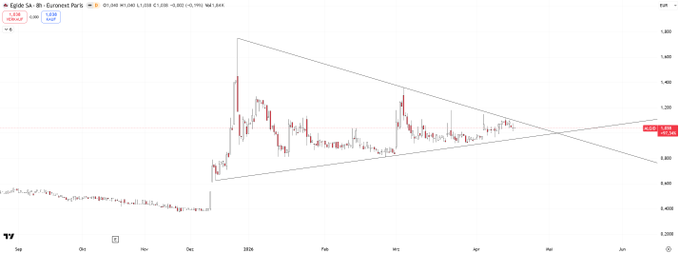
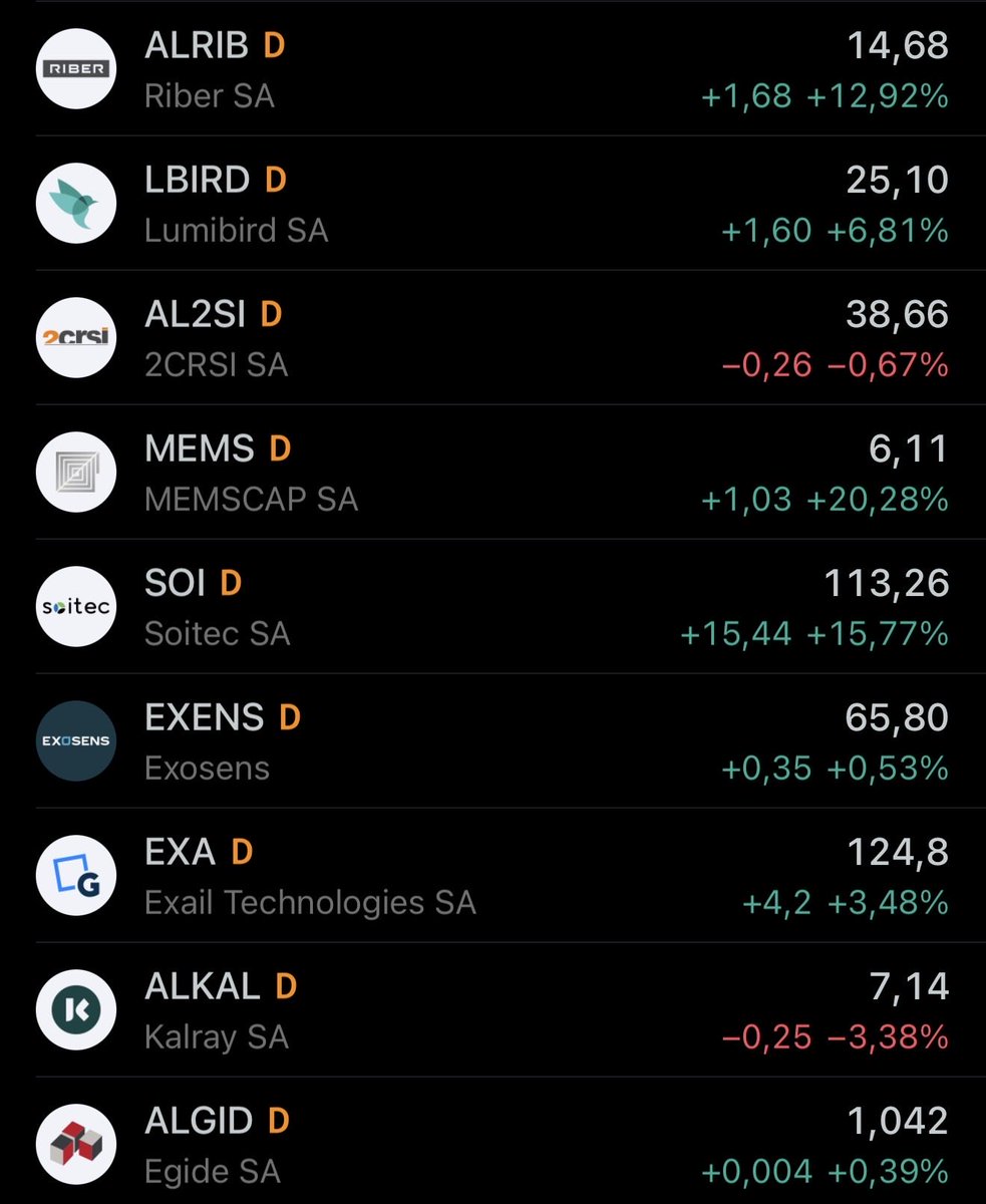
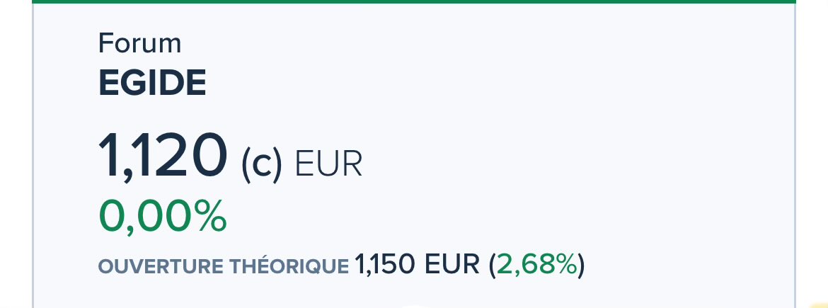
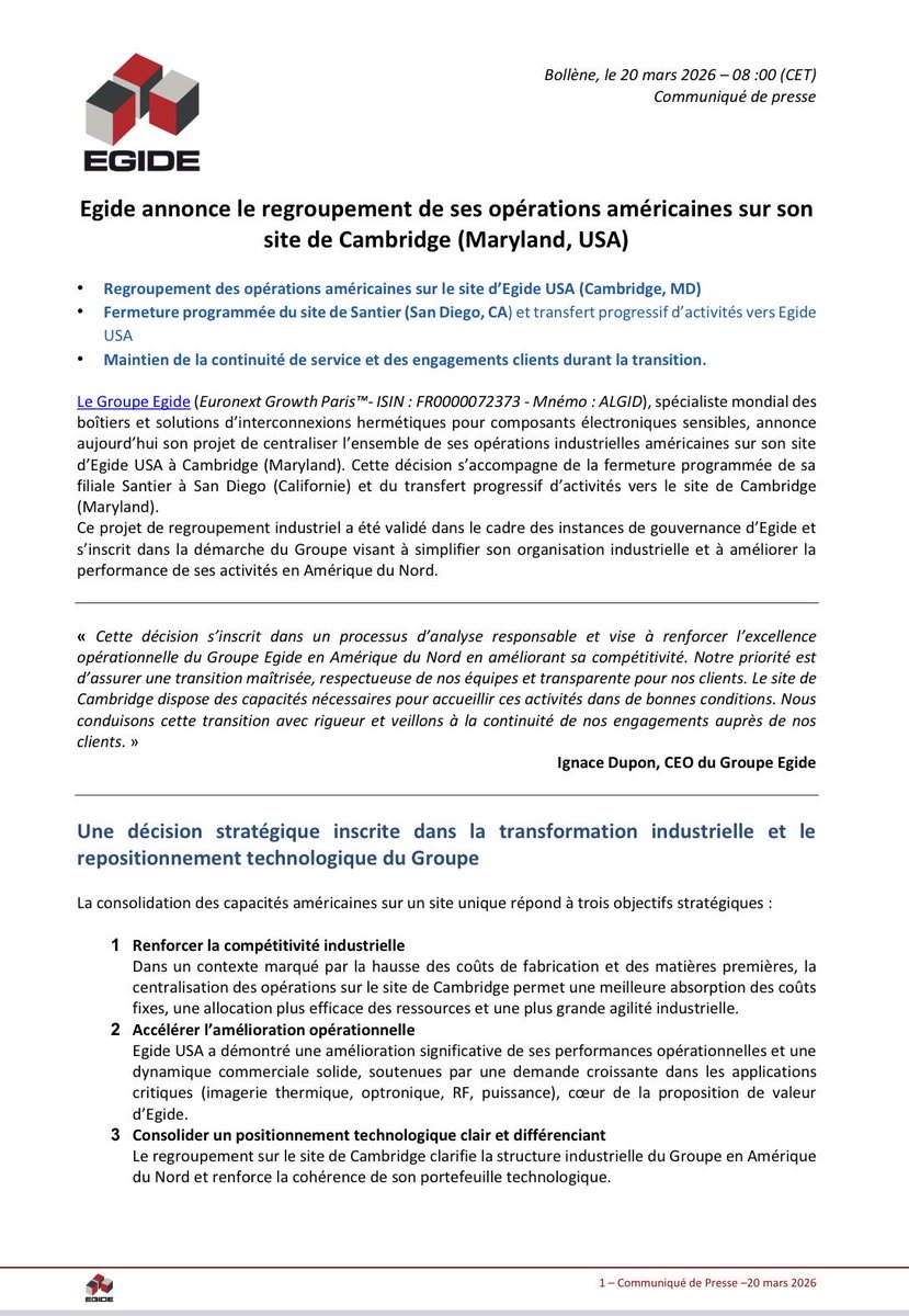
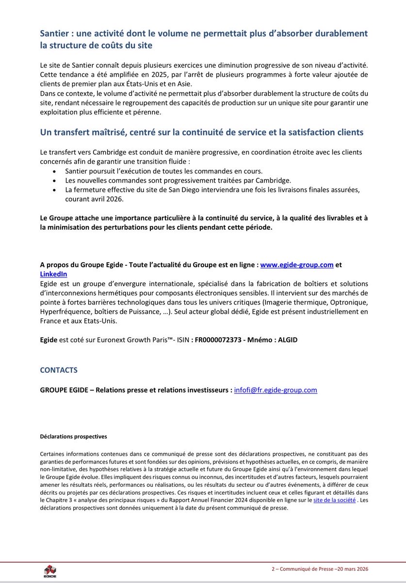
@BULLOFBRITAIN U forgot Egide $ALGID with 20M€ mcap also on euronext wich is a bigplayer in the photonic sector
English
🎲
323 posts


On Thursday/Friday I took starter positions in $LPK $M7U (Nynomic) $AIXA The equipment layer enabling AI's physical buildout is still mispriced relative to what it takes to actually ship 800G/1.6T optics, glass substrates, and GaN power for 800V racks. $AIXA: Aixtron controls 90% of InP MOCVD reactors globally. Every InP laser chip inside an 800G or 1.6T optical transceiver starts life inside one of their tools. NVIDIA's $4B investment into Lumentum and Coherent was the clearest possible signal that InP laser capacity is the real bottleneck of AI datacenter optics. TrendForce projects 800G+ transceiver shipments hitting 63M units in 2026 (2.6x jump). Every single one needs InP. Aixtron also holds 70-80% share in GaN MOCVD, directly levered to the 800V HVDC architecture $NVDA is pushing for next-gen AI factories. Management has guided to a doubling of optoelectronics revenue in 2026. This is a pure play picks and shovels exposure to the two biggest physical layer constraints in AI infrastructure, optics and power. $M7U (Nynomic): Holding company trading below book value at 1x sales. Market cap €70M. Inside sits LayTec, the quasi-monopolist for in-situ metrology on MOCVD epitaxy reactors. 90% share in InP datacom, OEM-integrated directly on Aixtron's G10-AsP platform as "LayTec InSide." Every Aixtron reactor shipped contains their tech. Proprietary nk databases built over 25+ years form the moat. The deeper angle: LayTec isn't just InP anymore. Since 2021 they've built an etch metrology platform (TRIton + Etchpoint) via a second OEM integration with Oxford Instruments, scaling across all III-V material systems including GaN power. 300mm GaN volume production hits 2027-2028, exactly when NVIDIA's 800V architecture goes mainstream. LayTec's standalone M&A value plausibly exceeds the group's entire market cap, everything else in the holding is being handed to you for free. The rest of the portfolio (tec5, Avantes, Sensortherm, Image Engineering) provides additional indirect AI photonics exposure via silicon photonics, CPO assembly, and plasma etch diagnostics. $LPK: Glass substrate play. Their LIDE process (laser-induced deep etching) is the technology leader for through-glass vias in advanced packaging. Management states 80%+ of the relevant industry players have already purchased initial equipment. Inferred strong customer links across Intel, Samsung SEMCO, LG Innotek, Unimicron, AGC, with Absolics looking increasingly plausible after their exclusive with F&S Electronics ended in March 2026. Intel patent filings describe a process that matches LIDE's exact two step architecture. Samsung electro mechanics reportedly teamed with LPKF + Chemtronics on TGV development, with TGV and plating developed inhouse using Applied Materials and $LPKF equipment per Korean reporting. Unimicron connection goes through JWMT (who source laser tech exclusively from LPKF) and have explicit co-development work with UMTC mentioned by JWMT's CEO. First ramp up orders have been booked in Q1 2026. CEO has reaffirmed 2027 as the ramp year. Also has exclusive CPO-on-glass development partnership with a US semiconductor company strongly inferred to be Intel based on timeline matching. Sourced alot of the info from: @vlmkapital @ParadisLabs @MoodyWriter13 So make sure you follow them too!

$33,000 in Sandisk 1 year ago is $1,023,000 today.


Pour un package global de 70 000 €, retenez que votre salaire mensuel net (fixe) sera d'environ 2 700 € net d'impôts (tranche jusqu'à 14%) pour une ventilation fixe-variable comme suit : 70-30. La culture de l'appauvrissement en France

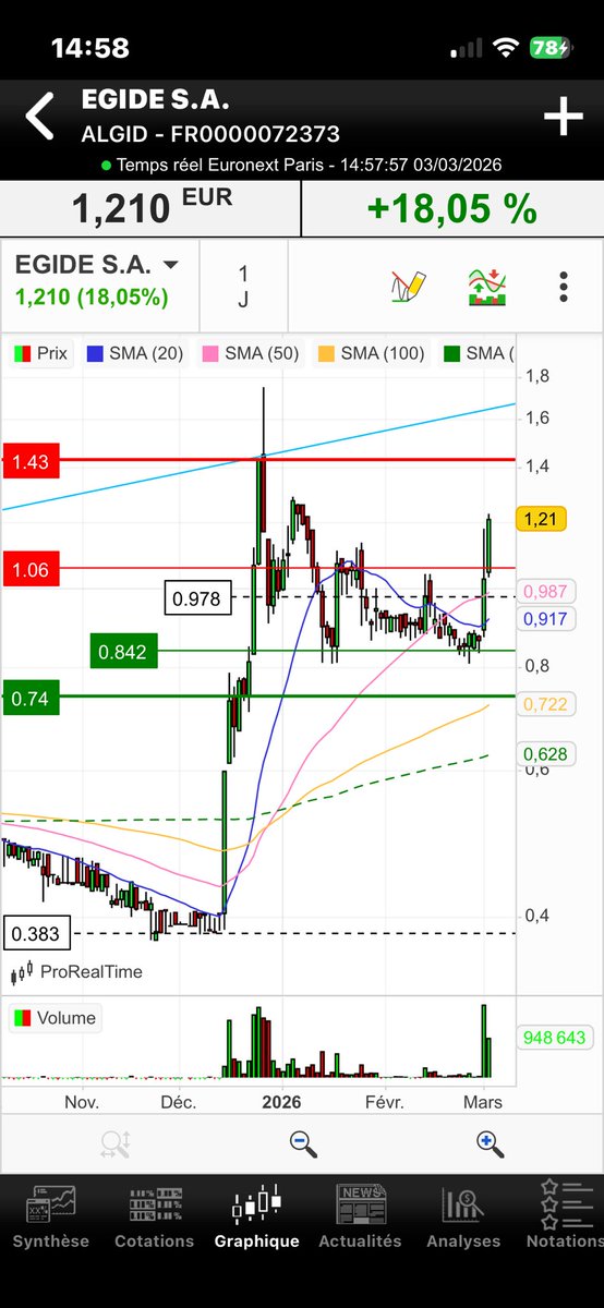
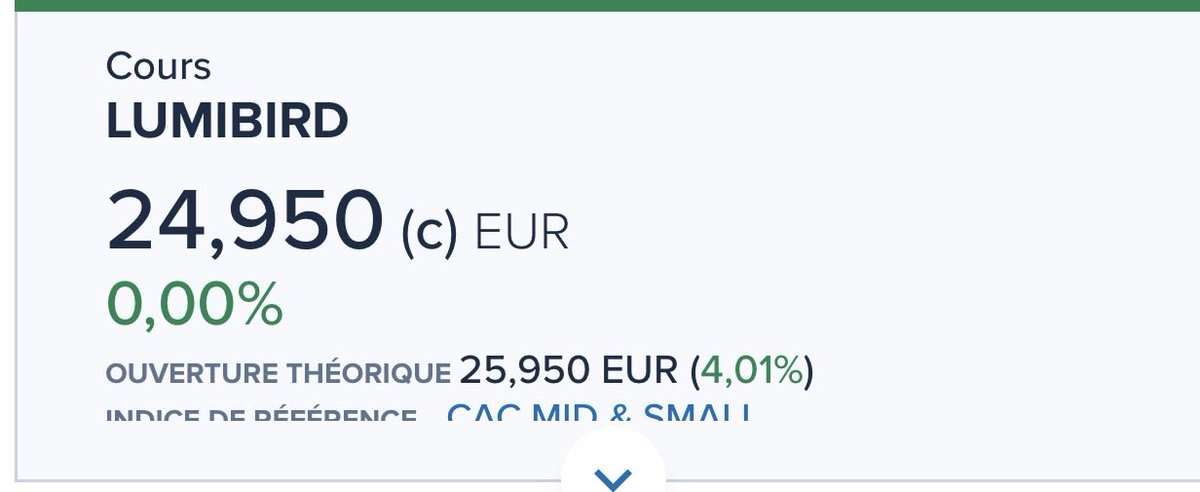
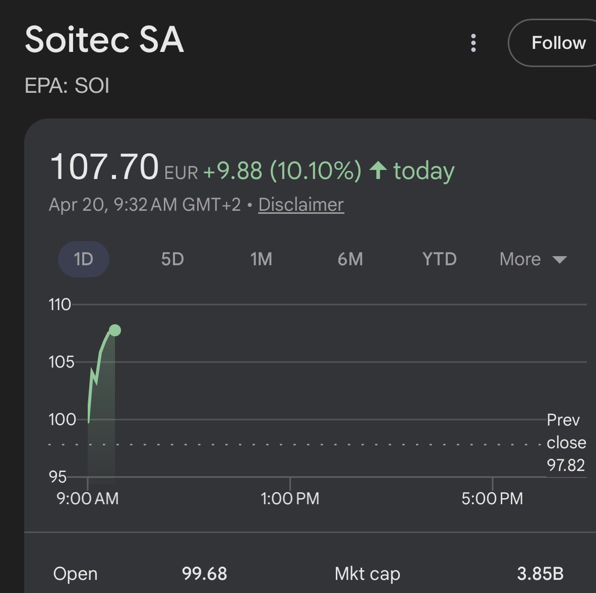
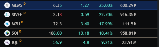
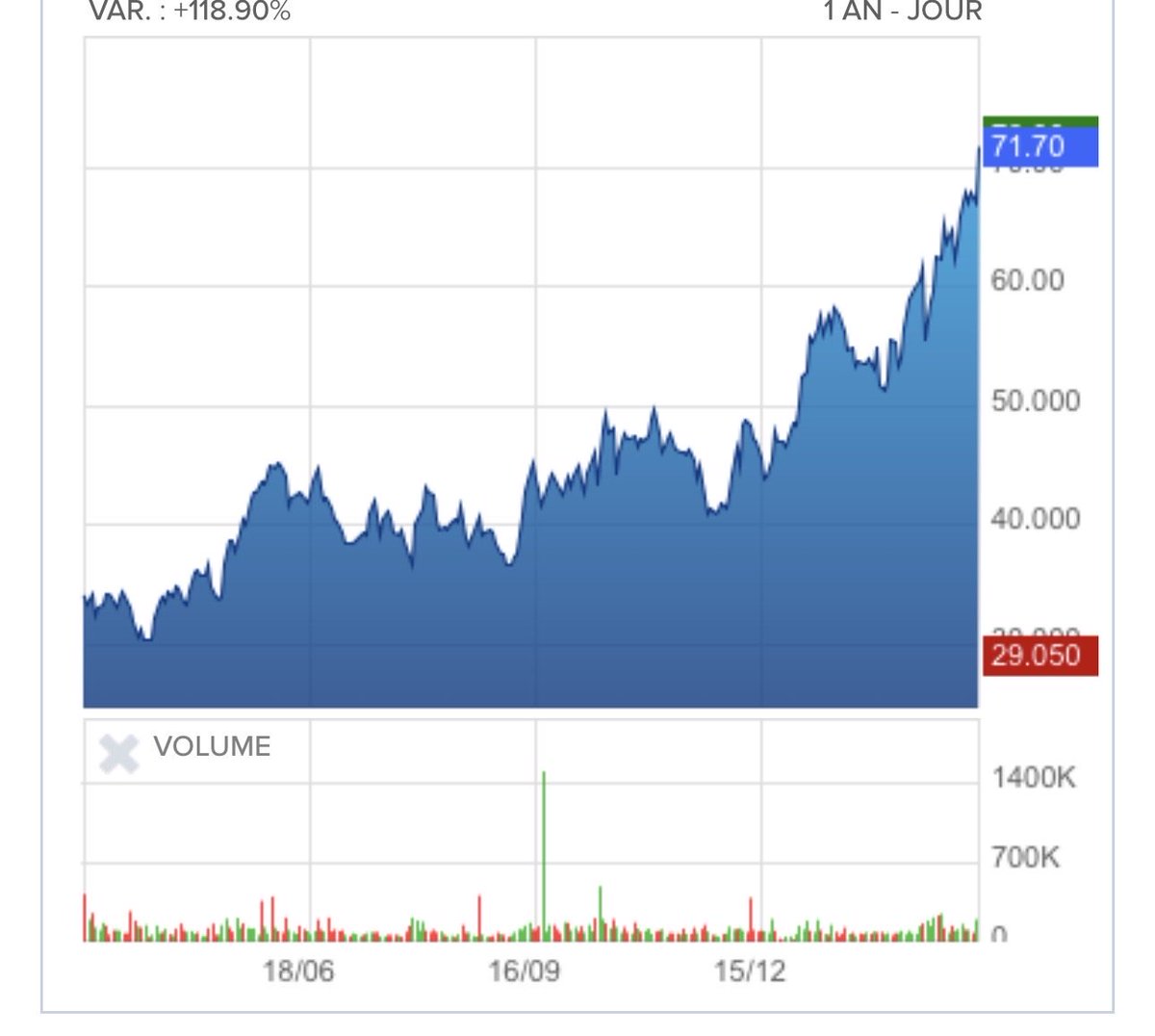
$ALGID Égide Group à surveiller +24% à 9h30.