Tim Bunce

21.6K posts

Tim Bunce banner
Tim Bunce

Tim Bunce

@timbunce

Somebody, and/or other.

Ireland, Rare Earth เข้าร่วม Haziran 2008
250 กำลังติดตาม1.3K ผู้ติดตาม
Tim Bunce รีทวีตแล้ว
Into The Forest Dark
Into The Forest Dark@ElliottBlackwe3·
The wisdom of Bill Watterson. This makes me think of Marcus Aurelius' words “Dwell on the beauty of life. Watch the stars, and see yourself running with them.” I am a firm believer in gazing upward, of being overcome with awe & wonder at the night sky.
Into The Forest Dark tweet media
English
29
397
2K
59.9K
Tim Bunce รีทวีตแล้ว
Into The Forest Dark
Into The Forest Dark@ElliottBlackwe3·
The older I get, the more I realize that it is not about what I accumulate but what I give away. Not just in terms of money or possessions, but am I generous with my attention to someone who needs it? Am I offering up my time, my gentleness, my compassion, my mercy & grace?
English
4
21
238
9.6K
Tim Bunce
Tim Bunce@timbunce·
Your task is not to seek for love, but merely to seek and find all the barriers within yourself that you have built against it. — Rumi
English
0
0
3
130
Tim Bunce รีทวีตแล้ว
Nautilus Magazine
Nautilus Magazine@NautilusMag·
How did society understand abortion historically? Claudia Ford, herbalist and midwife turned environmental historian provides us with a history lesson:   nautil.us/how-was-aborti…
English
0
4
8
2.3K
Tim Bunce รีทวีตแล้ว
Screen Ireland
Screen Ireland@ScreenIreland·
Do the bright lights, loud music and endless gift shopping of Christmas ever feel like.... too much? 🎄 You’re not alone – as the five characters of Ken Wardrop’s So This Is Christmas will show you. Discover their stories in a cinema near you: 🔗 wheretowatchireland.com/movie/so-this-…
Screen Ireland tweet media
English
5
11
101
917.2K
Tim Bunce รีทวีตแล้ว
Into The Forest Dark
Into The Forest Dark@ElliottBlackwe3·
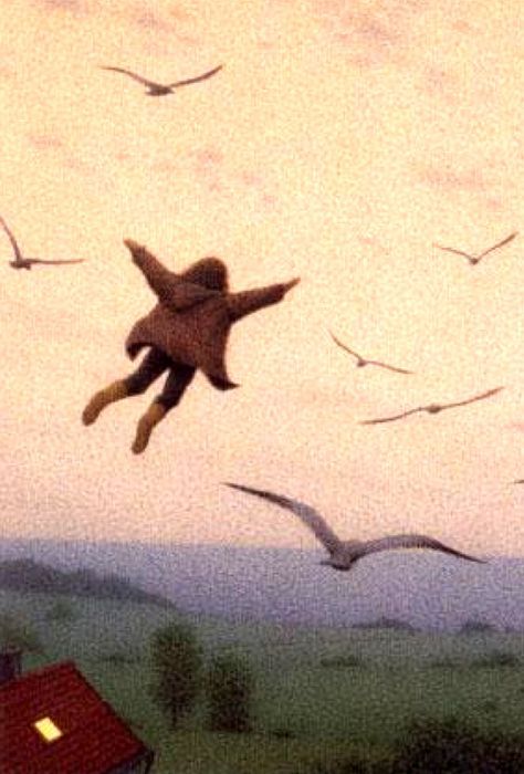
No matter what the world tells you, stay a dreamer. (art by Quint Buchholz)
Into The Forest Dark tweet media
English
3
141
775
30.4K
Tim Bunce รีทวีตแล้ว
Science girl
Science girl@sciencegirl·
A Tardigrade (Water Bear ) walking across a glass slide
English
298
2.6K
25.8K
2.5M
Tim Bunce รีทวีตแล้ว
Seamus Heaney
Seamus Heaney@HeaneyDaily·
Hope is not optimism, which expects things to turn out well, but something rooted in the conviction that there is good worth working for.
English
19
1.3K
4.3K
399K
Tim Bunce รีทวีตแล้ว
Craig Taylor
Craig Taylor@CraigTaylorViz·
A mash up of some 3d work over the past month or so for todays #30DayMapChallenge. It's a mix of work brand stuff, personal experiments and some abstract art exploration thrown in for fun. I also updated my website with some projects from this year mapzilla.co.uk if you want to see more 3d map fun! #3d #map
English
4
41
268
33.7K
Tim Bunce รีทวีตแล้ว
Atlas Obscura
Atlas Obscura@atlasobscura·
Originally commissioned as a sculpture to reflect the history of Belfast's red-light district, the final sculpture has been banned from Belfast public land. atlasobscura.com/places/monumen…
English
0
9
28
15.9K
Tim Bunce รีทวีตแล้ว
Saloni
Saloni@salonium·
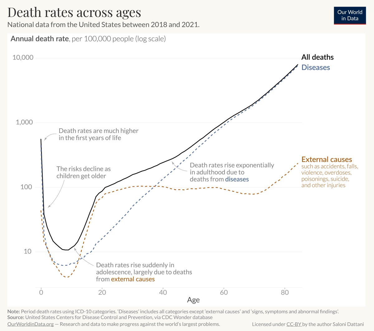
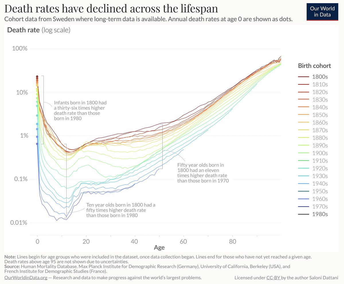
How do the risks of death change as we age – and how have they changed over time? I'll explain this with 4 very cool new charts below! ourworldindata.org/how-do-the-ris…
Saloni tweet mediaSaloni tweet mediaSaloni tweet mediaSaloni tweet media
English
1
10
34
4.9K
Tim Bunce รีทวีตแล้ว
Alec Stapp
Alec Stapp@AlecStapp·
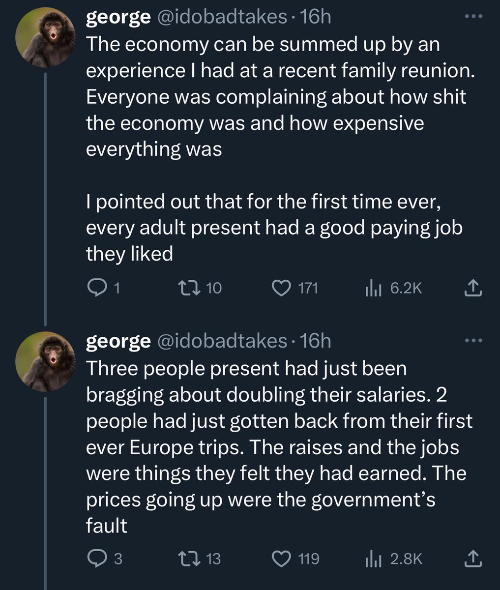
This might be the best explanation I’ve seen for the divergence between consumer sentiment and economic data @idobadtakes
Alec Stapp tweet media
English
96
904
5.1K
612.1K
Tim Bunce รีทวีตแล้ว
Historic Vids
Historic Vids@historyinmemes·
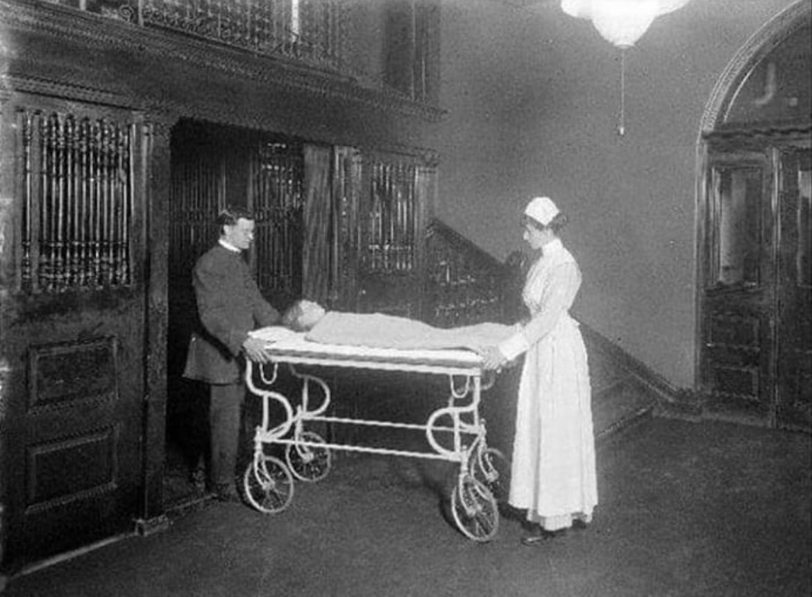
In 1922, a group of scientists went to the Toronto General Hospital where diabetic children were kept in wards, often 50 or more at a time. Most of them were comatose and dying from diabetic ketoacidosis. These children were essentially in their death beds, awaiting what was at that time, certain death. The scientists moved swiftly and proceeded to inject the children with a new purified extract of insulin. As they began to inject the last comatose child, the first one to be injected began to wake up. Then one by one, all the children awoke from their diabetic comas. A room that was full of death and gloom suddenly became a place of joy and hope. In the early 1920s, Frederick Banting and Charles Best discovered insulin under John Macleod at the University of Toronto. With the help of James Collip, insulin was purified, making it available to successfully treat diabetes. Both Banting and Macleod earned Nobel Prizes for their work in 1923. Banting was 32 when he received the Nobel Prize, and he chose to share half the prize money with Best, who was his assistant and just 24 years old at the time. Banting refused to put his name on the patent and instead sold it to the University of Toronto for $1. He thought it was unethical to profit from a discovery that would save millions of lives. "Insulin belongs to the world, not to me," he said.
Historic Vids tweet media
English
370
4.5K
24.7K
4.9M
Tim Bunce
Tim Bunce@timbunce·
Perhaps the secret of living well is not in having all the answers but in pursuing unanswerable questions in good company. – Rachel Naomi Remen #q
English
0
0
0
99
Tim Bunce รีทวีตแล้ว
Christian Keil
Christian Keil@pronounced_kyle·
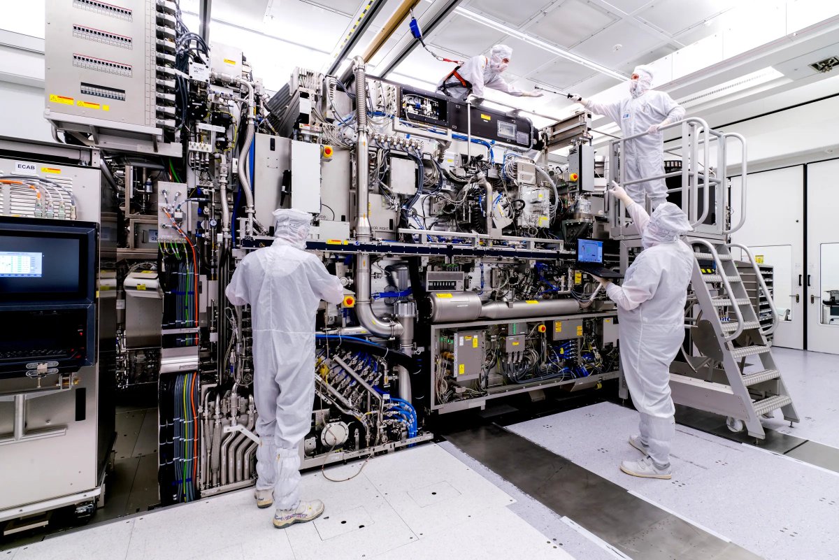
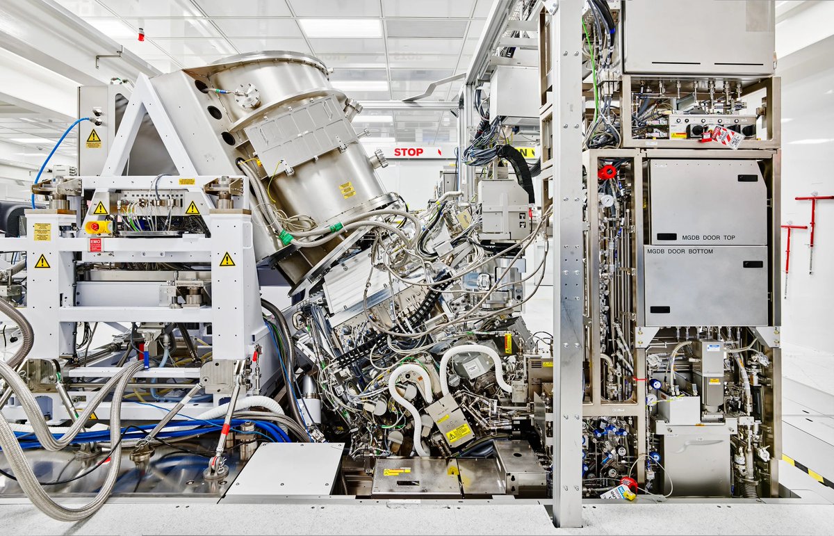
I love Twitter — after posting about TSMC last week, a former ASML technician reached out to me... His name is Daniel Hatton-Johnson, and he shared a bunch of cool behind-the-scenes stuff that you can only really learn by living it. I asked, and he agreed to let me post his message in full: Hi Christian, I saw your Tweet on TSMC and why what they do is so hard. There were so many good answers and recommendations. Background The reason I thought to write is that I have lived in Eindhoven in the Netherlands for the last four years. I came to start a deep tech company at an incubator here (another story). On arrival in October 2019 I had no manufacturing or production experience at all, so I got a part time evening job at ASML whilst working on the company. Then the following year moved to a company called SMART Photonics, who make Photonic Integrated Circuits. A relatively tiny semiconductor company, that has raised around €100 million to date. I’ll mostly summarize those experiences below. I currently work as a Quality Technician at VDL Enabling Technologies Group, where we make some of the smaller machines and modules that go inside the giant ASML machines. This includes the vessel, which is the thing that vaporizes the tin droplets to generate UV light. I literally work with those and two other machines every day, the atmospheric wafer handler and the vacuum wafer handler. ———————— Eindhoven eco system One thing to note is that all of these companies came out of Philips, what was originally a lighting company before electronics and now mostly advanced medical equipment. Eindhoven is named the city of light. Not because of light bulbs, but because there was a huge match industry from the 1840’s to the 1920’s. Both ASML and SMART spun out of Philips, whilst VDL ETG was an acquisition by the VDL Group, a large Dutch industrial family business that also started as a single machine shop in Eindhoven in 1953, which included Philips among its first clients. I gave this background because it gives some insight into the size and depth at least one chip making and industrial eco system here. For a long time it has attracted engineers, scientists and technicians from around the world. Then you have a very large supply chain to be able to build things and so it's easy to create companies that build things or service the companies that are building physical products. From basic things like chains, hoses, tractors and ceramics to advanced cooling, lasers and medical equipment. Another fun fact is that Eindhoven has the highest concentration of patents per head of any city in the world. It also has the, by far, highest concentration of people with autism in the world as invention, autism, creativity and things like left handedness have been shown to be correlated. With the children of doctors and engineers the most likely to score highly for neurodivergent traits. ———————— Companies ASML - I worked a basic technician job in a cleanroom of the servicing building so won’t elaborate too much there. We basically used to check and ship parts to fix machines that were installed globally. VDL - I work on the two wafer handlers, the vessel and their spare parts. This role is fairly advanced manufacturing, but it's not too hard or intricate in comparison to making chips. The harder part is the design, iteration and prototyping when a new version of a machine gets built. Thereafter its a fairly steady, standardized process. It then goes to ASML where they have to get those things working to spec which is pretty hard as it requires small tolerances that rely on great software to get all of the moving parts talking to each other. That’s where it really becomes rocket science again. SMART Photonics - They are a foundry making tiny photonics chips. These chips are still relatively large compared to modern electronic integrated circuits. The reason being that light has a much longer wavelength than electrons do. The wavelength of light used in PICs is typically between 1500 nm and 1650 nm. This means that the features in a PIC must be at least as large as the wavelength of light in order to effectively guide and manipulate the light, always following a curve to take a smooth path and prevent reflection. In contrast, electrons have a much shorter wavelength, on the order of 0.1 nm so the feature size can get tiny. Meaning that the process is not just intricate, it’s unimaginably difficult to do and then to scale and have good yields. Any contamination like a tiny grain of dust on any layer can damage and destroy a photonics chip, and that same particle that would leave a photonics chip functional would likely destroy an electronic chip or two with such small feature sizes. Much of our process was still similar and because of the larger feature size and being a lab to fab rather than a full chip fab, we did more experimentation and more manual handling than you’d ever see in a large scaled up electronic semiconductor plant. So you got to see a wafer start from the beginning, blank and then see layers added, or removed and transformed by the process. The base material for our foundry was mostly indium phosphide (InP), and sometimes gallium arsenide (GaAs) rather than silicon since as both materials are able to generate light. Though InP for example has comparatively high loss, compared to Silicon since it's such a great insulator meaning light propagates well though silicon waveguides. But they then need an external, usually larger light source. With InP that can all be done on chip and [we were all in] on InP. Though the drawbacks are that the material is very brittle and the process is still not scaled like CMOS so we started with two and three inch wafers. The company has now moved to four inch wafers so with larger chips and smaller wafers, the yields don’t come anything close to electronic chips which tend to be about 12 inches across. So the costs are relatively high, but the applications such as quantum computing, sensing and detection cannot be done in silicon electronics, adding massive value to the areas where these chips are used. As with silicon the production of a single finished wafer takes around 8-16 weeks and on the way there, there could be any number of challenges because you are using machines and materials that are undergoing nanoscale state changes. So for examples you may change the formula or your photoresist, or you could have two materials that interact well until there are changes in temperature with heating or cooling from the bake off process for example. Which could leave cracks in a layer of your chip because the materials could expand or contract at different rates or temperatures whilst being structurally connected. Any metal or glass/silica waveguide on top of this could then have a short circuit in the electronic components and loss or scattering in the photonics components. So you’d grow layers of InP in a huge reactor, do chemical etching, photolithography and a number of different process steps, adding and removing materials, building a working chip layer by layer. The amount of processes involved are staggering. There are reactors for crystal growth which need to be connected to dangerous gases. This for us was generally done by experienced engineers and chemists/materials scientists who would go into those rooms with masks and oxygen tanks on. Then you have machines for photolithography that we mostly got from ASML. These didn’t need to be top of the line due to larger feature sizes so we had older machines as they last a very long time. Then a newer one which is relatively cheap in the low tens of millions of euros. Add to that ultra precise measuring and metrology equipment, SEM microscopes and other microscopes of varying strengths. The list of high tech machinery was endless. This all had to be maintained by experienced process engineers and technicians. ———————— The people This is a summary of my experience as someone who was previously a layperson and went head first into this environment after a life of office work. I have a degree in sociology and did further study later in things like UX design and other things in digital and IT. Coming here was an expansive, mind bending experience. It’s like a totally different world compared to most cities. I spent lots of time speaking to my colleagues and so many of these people were just incredible. They’d have to solve impossible problems constantly under pressure, in the middle of a batch that if ruined would take weeks to get back to the same place. You could grab a colleague in the lunch room and ask anything about their area of expertise and the depth of knowledge and experience was generally unbelievably high. If you didn’t want to talk about work it could be a conversation about time dilation or any number of things related to the sciences as they are, or going over outstanding questions in science. For some time I sat next to a guy who was a brilliant mathematician, trying to solve Goldbach's conjecture in his spare time. He believed only prime numbers were truly numbers as opposed to base 10, or base 12 number systems which as he said were largely culturally defined and arbitrary. That guy was incredibly interesting, as were many people there. The guy who swapped desks with him was trained in chemical engineering and was equally brilliant. These were two middle aged white guys who wore glasses and had a kind, calm demeanour, which makes you stop believing in both ageism and talented assholes as a pathway to success. With companies like ASML and TSMC, they have many, many more of these individuals. In fact some of our best people had come from ASML and the large chip companies like NXP. But they generally wanted more freedom, creativity and a better work life balance as the big companies require a lot of overseas travel. Those people work under immense pressure and are pretty well compensated for it. This is mostly personal experience and it’s a little short, but I wanted to at least give some insight from one part of the global semiconductor ecosystem here in Eindhoven. I’d be happy to either talk a little more, or try to put you in touch with a colleague or former colleague who knows more. I also have a friend working at Schunk Xycarb in the next town over, which is a company specializing in Carbon manufacturing at scale. They grow the large crystals that become the wafers for semiconductor, which again is a highly specialized process in itself. This whole thing is a huge, huge ecosystem, and the fabrication of chips, the epicenter of it, is probably the hardest part along with creating and operating the lithography machines at scale in a way that generates profits. I have missed entire areas like mask design, testing, reliability testing, logistics, transportation design, and delivery processes for multiple customers.
Christian Keil tweet mediaChristian Keil tweet media
English
37
314
2K
348.8K