
It’s wild that the most profitable webpage on the internet is made of a textbox, one useful button, and another useless joke button. And it hasn’t changed in 20 years.
Equity
4.9K posts

@equityst
In deep love with tech 💻, startups 🛠 and the visionary founders 🧙 making magic happen ✨ Super tiny angel investor in 2 startups 🤩

It’s wild that the most profitable webpage on the internet is made of a textbox, one useful button, and another useless joke button. And it hasn’t changed in 20 years.


Photonics is a bit confusing, hopefully this simplified summary helps. I have positions in $TSEM, $SOI, $ALMU, $LPKF

$HIMX partner Foci just presented at BofA Asia tech (3/20/26 am local). Great stuff in here. >5 potential customers, including possibility of 1.6T and 3.2T and scale-out in addition to scale-up. The prize is >6.4T presumably Nvidia. Potential customers high % since via COUPE


People can guess why PlanOptik would be invited to and participate in a conference focused on hybrid bonding $P40


유리기판 독점과 모트 분석 | 260413 유리기판은 AI 반도체 시대의 핵심 소재임. 기존 플라스틱(PCB) 기판 대신 유리를 쓰면 신호 손실이 줄고 열에 강하며 더 미세하게 회로를 새길 수 있음. 그 유리를 만들고 가공하는 기업이 $GLW $AGC $LPKF 세 곳임. 1. 유리기판이 뭔지부터 알아야 함. 스마트폰·PC 안에 있는 반도체 칩들은 기판 위에 올려짐. 기존엔 플라스틱 소재 기판을 씀. 근데 AI 시대엔 칩이 훨씬 빠르고 촘촘해야 해서 유리 기판이 필요해짐. 유리는 평탄도가 높고 열에 강하며 미세 회로를 더 정밀하게 새길 수 있음. 2. $GLW 코닝은 170년 된 소재 회사임. 흔히 아이폰 화면 유리 '고릴라 글라스' 만드는 회사로 알려져 있는데 그 깊은 소재 노하우가 반도체 유리기판에도 그대로 적용됨. 수십 년간 쌓은 유리 배합 공식과 제조 공정 데이터는 돈 주고 살 수 없는 자산임. 3. 코닝의 '퓨전드로' 공정이 핵심 moat임. 퓨전드로는 유리를 V자 홈에 흘려보내 양쪽으로 흘러내리게 해서 대형 초박형 유리를 뽑아내는 독자 공법임. 이 설비를 짓는 데만 수천억 원이 들고 노하우 없이는 안정적인 품질을 내기 어려움. 경쟁사가 따라 하려고 해도 최소 10년은 걸림. 4. $AGC 일본 AGC(구 아사히글라스)도 만만찮음. 반도체 공정에서 칩과 유리의 열팽창률(CTE)이 맞지 않으면 금이 감. AGC는 이 CTE를 실리콘과 유사하게 맞춘 '알칼리프리 유리'를 다양하게 공급함. 얇기 0.2mm부터 다양한 사이즈까지 커스터마이징 대응이 강점임. 2025년에는 AR·MR 글라스용 고굴절 기판으로 CES 혁신상까지 받음. 5. 유리기판엔 구멍을 뚫어야 함. 반도체 회로를 연결하려면 유리에 수십 마이크로미터(머리카락 굵기의 1/10) 수준의 구멍을 정밀하게 뚫어야 함. 이걸 TGV(Through Glass Via)라고 부름. 유리는 플라스틱보다 훨씬 딱딱해서 이 작업이 엄청나게 어려움. 6. $LPKF 독일 LPKF가 TGV 가공 분야를 장악함. LPKF가 개발한 LIDE(Laser Induced Deep Etching) 기술은 레이저로 유리 내부에 손상 흔적을 만들고 이후 화학 식각으로 깔끔하게 구멍을 뚫음. 균열 없이 정밀한 구멍을 낼 수 있는 유일한 방법에 가까움. 2025년 한국 특허도 취득해서 IP 보호가 더 강화됐음. 7. LPKF의 한국 시장 점유율이 약 80%에 달함. 삼성전자 SK하이닉스 같은 대형 고객들이 시제품 라인에서 이 장비를 쓰고 있음. 장비를 한번 도입하면 공정 전체가 그 장비 스펙에 맞춰 설계되기 때문에 쉽게 바꾸기 어려움. 이게 이른바 '고착(lock-in)' 효과임. 8. 특허와 노하우가 신규 진입을 막음. $GLW 의 퓨전드로, $LPKF 의 LIDE 모두 핵심 특허로 보호됨. 여기에 수십 년의 제조 경험과 불량률 관리 데이터까지 더해지면 신규 기업이 진입하는 건 거의 불가능에 가까움. 돈만 있다고 할 수 있는 게 아님. 9. AI 반도체 수요 폭증이 이 moat를 더 굳건하게 함. 인텔·AMD·엔비디아가 모두 유리기판 도입을 검토 중임. $GLW 는 메타와 60억 달러짜리 장기 계약을 체결했음. 수요가 폭발적으로 늘수록 먼저 대형 고객을 잡은 업체가 기술 피드백을 먼저 받고, 제품을 더 빨리 개선함. 선두 기업이 더 앞서나가는 구조임. 10. 2027년 본격 양산이 진짜 분기점임. 현재는 아직 시제품·평가 단계임. $LPKF CEO는 2027년 양산 시작을 전망했고, 자동화 장비 공급까지 준비 중임. 유리기판이 상용화되면 이 세 기업은 수년 치 선점 효과를 누림. 지금이 구조적 moat가 완성되는 시점임.

It's pretty interesting that the whole glass substrate supercycle essentially hinges on $LPK/ $LPKFF –a <€200M market cap company from Germany Glass is hitting an inflection point and the supply-chain is gearing up. Intel spent $1B+ on it. Samsung is sampling Apple. Absolics built a $600M fab in Georgia. LG Innotek is building pilot lines. Corning, AGC, SCHOTT are all supplying the glass 
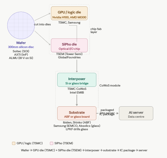
Capex is ramping and glass looks imminent (it is) to become the base material for the next generation of leading edge semi packaging–however if you dive deeper down the rabbit hole, you’ll quickly notice that glass substrates are useless without Through-Glass-Vias, tiny microscopic holes that carry electrical signals through the glass. No TGVs, no glass substrate, no party. It's literally just a piece of overengineered glass without them That leads us to $LPK. Let me give you the surface level overview of the thesis: TGV is hard. Glass is brittle. Traditional drilling can leave micro-cracks, rough edges and stress on the glass. This can hurt reliability and lower yield which directly leads to reduced margins $LPK does things a little different. They invented a two step process which uses a laser to modify the internal structure of the glass–then a wet chemical etching process which dissolves the modified regions. No micro-cracks, defect-free holes and sub-micron precision. This process is called LIDE (Laser-Induced Deep Etching) and is currently being adopted by ~80% of the glass substrate market for their qualifications Here is the overview: - $INTC: glass substrate packaging for 18A/14A, Clearwater Forest - Samsung Electro-Mechanics: sampling Apple and Broadcom, 2027 mass production - Absolics: first CHIPS Act recipient for glass, ramping production in Georgia - $011070/LG Innotek: pilot line, partnered with UTI, targeting 2028 - $GLW: supplying substrate-grade glass compositions - AGC, SCHOTT, Nippon Electric Glass: same All of these companies are betting their next-gen packaging roadmaps on glass. $LPK holds 80% market share in qualification with a long-term goal of maintaining 70% market share once HVM starts. Based on the list above, I'll let you take a guess who will, and won't depend on $LPK moving forward


