
Buko
143 posts

BREAKING: SpaceX is reportedly to publicly disclose its IPO prospectus filing as soon as next week, per CNBC
English
@ARealRocketMan @_MaxQ_ Yes, it is crazy. I remember watching the water tower launch years ago. This was an insane idea at the time. Amazing what @elonmusk and the team achieved.
English

Starhopper was SpaceX's first low-altitude prototype for the Starship program, built in early 2019, to test the Raptor engine and landing systems. The vehicle successfully completed two "hops," culminating in a 150-meter flight in August 2019.
Starship is has taken quite a "leap" forward technologically in six short years. Imagine what the next six will bring. Congratulations team @SpaceX .
📷Credit: @SpaceX

English


Starship launch next week!
SpaceX@SpaceX
Starship’s twelfth flight test will debut the next generation Starship and Super Heavy vehicles, powered by the next evolution of the Raptor engine and launching from a newly designed pad at Starbase. The launch is targeted as early as Tuesday, May 19 → spacex.com/launches/stars…
English


@bubbleboi Well, it is good news, but the PC market is not driving this stock so high. AI does, but I agree with the flood of positive news, it is rare and has some downsides too.
English

I can’t believe this is my life.
Intel@intel
We're thrilled to partner with @Google on something we've been building with them - Googlebook. Premium, powerful devices designed for Intelligence. We can't wait to get it into your hands this fall. Learn more at ms.spr.ly/6013vuzjt #Googlebook #NEXT #Intel
English
@awakenowzone x.com/i/status/19499… Before Trump, but I'm just a nerd. Entered at 19. To me, it was obvious Intel was way undervalued and an easy entry.
Buko@Buko15815825
@AprendidoEs @Silicon_Fly Time to buy!
English

We need a list of analysts that recommended buys on $INTC BEFORE it was popular… say in the $20’s. How do we get that list?
𝘾 𝙃 𝙊 𝙇 𝙀 𝙑 𝙊 𝙑 𝙊 | LongINTC 🇺🇸🤖🚀@cholevovo
No.1 Intel $INTC
English
@stockdatamarket I don't know what LLM you are using, but mine said this price is about 40% probable before it happened and even beyond this price. It accounts for the news, not raw data.
English

Intel hit $112 today after an insane 185% rally.
The probability of $INTC reaching $112 was just 0.0172%.
For comparison, the odds of being dealt a Blackjack are about 2%, meaning Intel hitting $112 was roughly 100x less likely than pulling a Blackjack at the table.
Even getting Blackjack twice in a row was still more probable than $INTC hitting $112.
Absolutely historic move.

English
@MukkyunGovernor @lafaiel @hardwarecanucks Dell's long battery life is due to screen technology, not just Panther Lake. It's the same as the long battery life of a fanless Mac, which also conserves battery. The laptop is a whole piece.
English
@MukkyunGovernor @lafaiel @hardwarecanucks Apple is soo smart it must be in the design... Or Apple E core cant handle a task load and P core has to do the job. Think, not guess.
English

Dell XPS 14. 43 hours of battery life. 🤯
But would we recommend it over the MacBook Air M5?
Find out here - youtu.be/YgnVgVYOqbo
YouTube

English
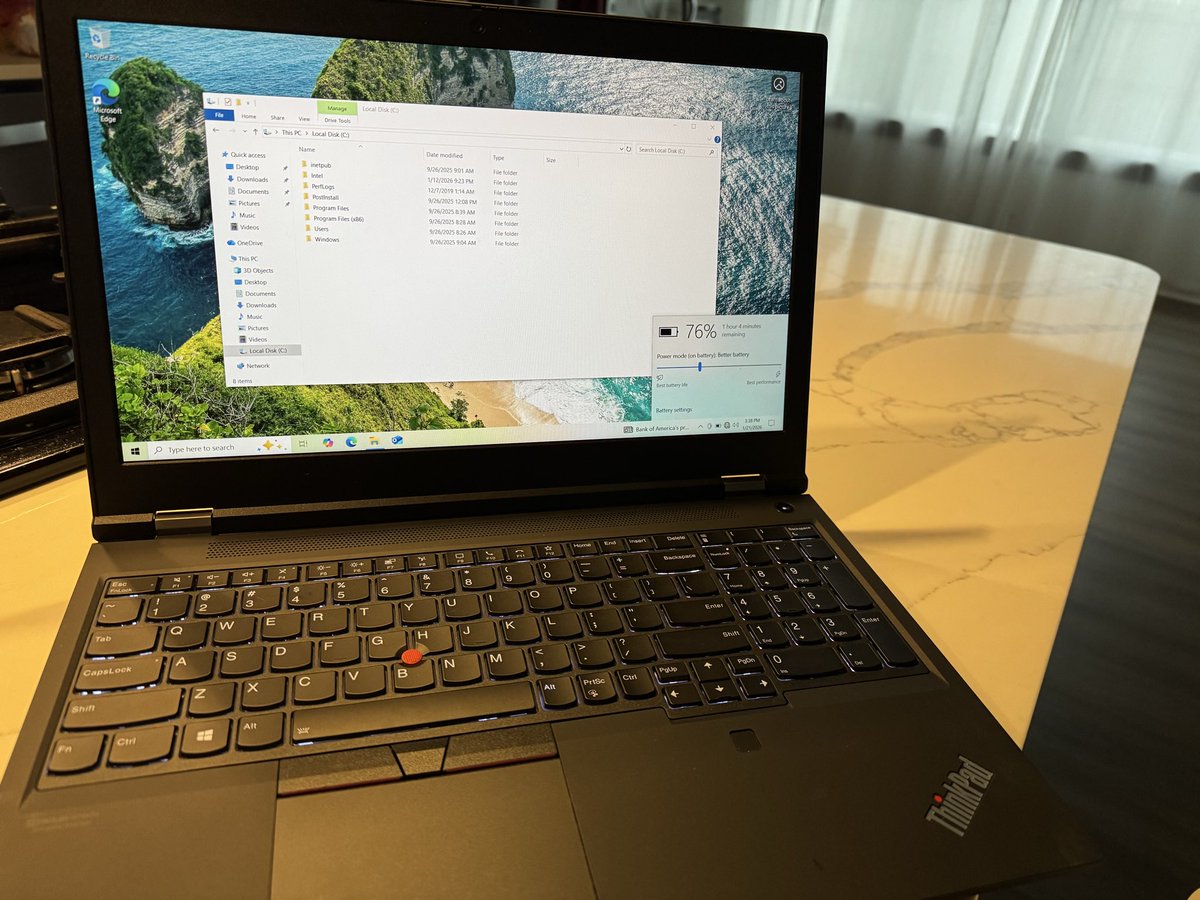
@realcatsalmon @folaoftech I also bought a ThinkPad for myself, just from work experience. When I touch this keyboard, working on it is an automatic experience.
English

@folaoftech I actually bought one of these mfs for my side hustle , bc i knew i would use it and work my ass off on my own shiet during my professional job’s over time, night shifts, day shifts, holiday shifts and even vacation 🤣
English

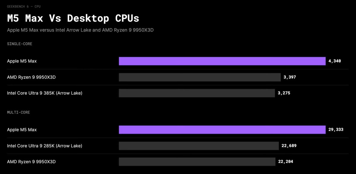
@SebAaltonen 385K single core and 285K multi core hmm ..? 385K will be more like ~3520 single-core and ~36080 multi
English

The first M5 Max CPU benchmarks look promising. M4 Max already had a notable ST advantage over desktop CPUs. Now the MT performance is clearly ahead of 9950X3D too. Tiny efficiency cores are gone. Now M5 Max has 6 super cores + 12 performance cores (18 total). It's a MT monster.
English
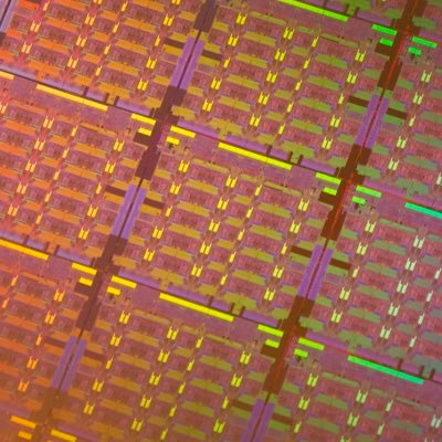
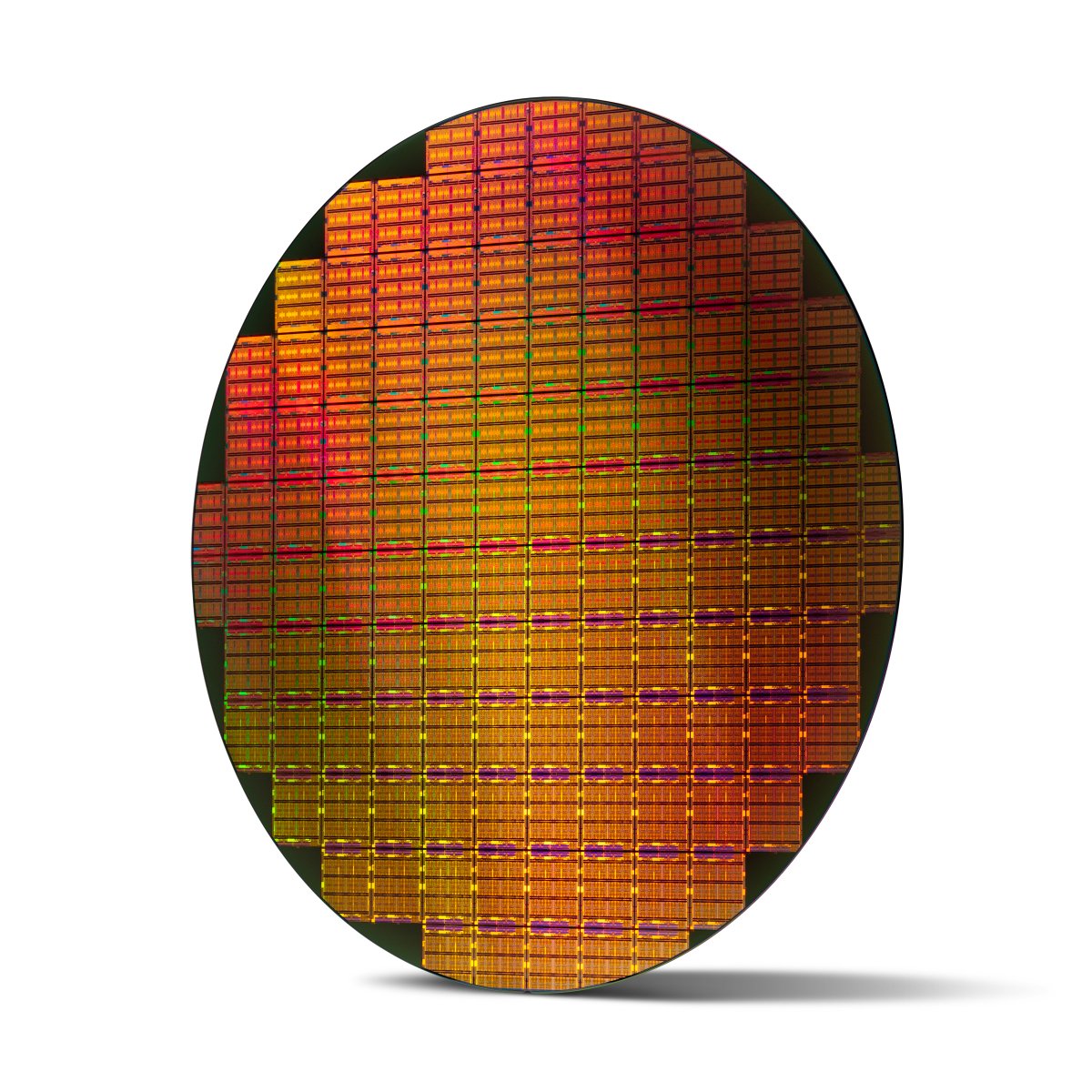
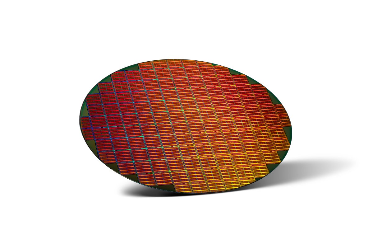
Intel just released some new wafer shots of Xeon 6+ aka Clearwater Forest with a different esthetic compared to what we have seen before. Thats presumably because more metal layers are present to this one?
English

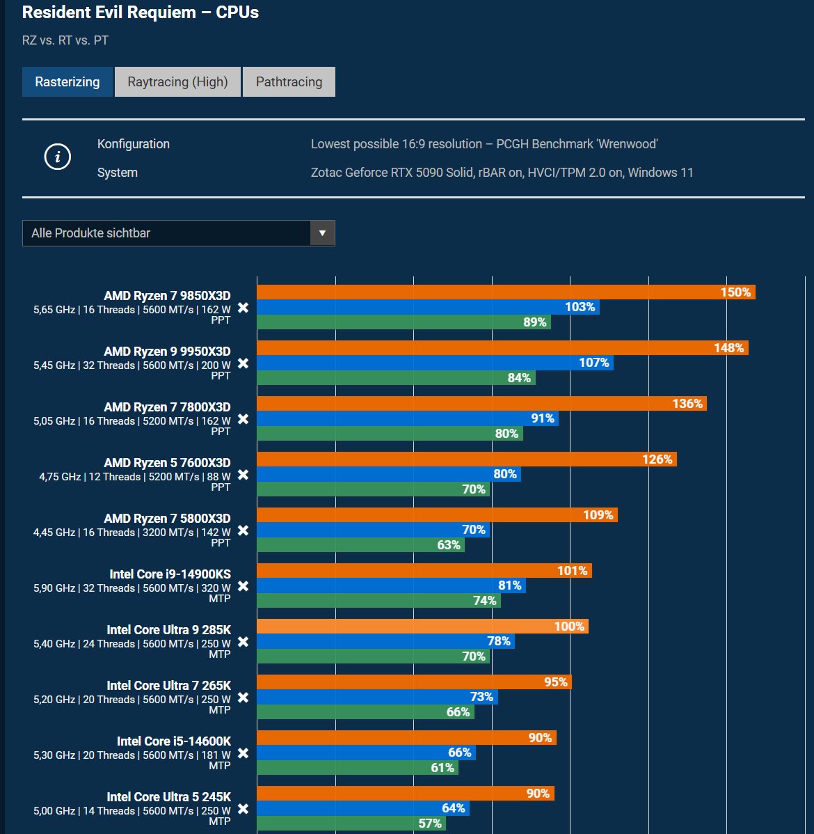
Resident Evil Requiem
The gap between Intel's best gaming CPU and AMD's best gaming CPU is ~50%......
pcgameshardware.de/Resident-Evil-…
English
@UniverseIce 80%? Under 30 minutes? Does it even hold longer at 45W than the previous models, 60W for 10 min? That is decent, not super.
English


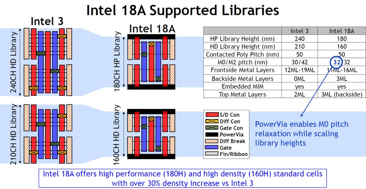
@D_K_Rajasekar It's literally written on the slide. "PowerVia enables M0 pitch relaxation while scaling library heights." Most importantly, "over 30% density increase vs Intel 3" - I think that matters more than any metal pitch dimension...
English

So Intel was able to print M0 pitch of 30nm in Intel 3 FinFet & was able to yield large dies for Xeon 6 but now struggling with M0 pitch of 36nm to yield small PTL 18A dies 🤔!? or was it a just design choice for PTL? or did Powervia work too well they relaxed it further?
Jukan@jukan05
To put this simply: 1. Intel's Marketing vs. Reality Gap Is Exposed Intel claimed 18A would offer 32nm M0 pitch, but the first actual production product uses only 36nm HP cells, with no HD cells at all. Intel's claim was that a single EUV exposure could achieve 32nm, yet it appears yields aren't even there yet at 36nm. For Intel, this is a rather disappointing start. 2. On GAA The logic GAA pitch comes in at 76nm — significantly larger than even SMIC N+3's fin pitch of 32nm. The author's key point is that GAA is actually a technology that relaxes lithography constraints, and yet Intel still can't get it right. This means the difficulty in semiconductors isn't just about EUV equipment. Process integration capabilities — etching, deposition, cleaning, etc. — are what truly matter, and this is where TSMC genuinely leads over Intel and Samsung. 3. The transition from 18A to 14A introduces BSCON, enabling backside power delivery even for SRAM. Meanwhile, Samsung's SF3 doesn't even have inner spacers — highlighting the technology maturity gap across foundries. (In some areas, Intel's technology actually leads Samsung.) Summary: - Intel Foundry's prospects for winning external customers look even bleaker. If they're still ramping yields on easy HP cells for their own products, it's hard for external customers to place their trust in Intel. - TSMC's technological moat is reaffirmed. The gap in process integration capabilities is clearly manifesting not just in node naming, but in actual production pitch and cell composition.
English
@7742_friedegg @AaronZ38425048 @hmph29759351 @ExoticSpice101 Becouse it is not easy to beat ARM core with x86 in power efficiency just using only better node.
English

@AaronZ38425048 @hmph29759351 @ExoticSpice101 If 18A was so good to use, why is even X9 388H having P4+E12?
Note: E12 = E8+E4.
English

Nah. I thought 18A/18AP had unquestioned leadership.
The reality is it’s not better than N3P or N2. Don’t believe this Intel driven propaganda account.
meng@meng59739449
looks like many people was semiconductor expert don't forget boast about N3B use mature FINFET Node , after N3E SRAM and transistor gate pitch relax and reduces EUV layers , 8% less density than N3B cost , yield , complexity need compromise 18A also same x.com/jukan05/status…
English
@ExoticSpice101 TSMC is undoubtedly the king of FinFET. Will it hold onto its edge with GAA future nodes? Time will tell.
English
@ExoticSpice101 Intel 18A has one major advantage over N2: wafer price. You can add government support and second-sourcing backup for big brands, and U.S.-based production, shifting to an open-fab business. It's a competitive node. Let's see if TSMC can deliver their slides in a real N2 product.
English
@ExoticSpice101 N2 is denser than 18A. TSMC is still the best here. Demand is so high that customers can't ignore 18A. Price and time to market also matters. 18A-P is a client-oriented node and has ~10% better performance than 18A. I rank them N3(X) < 18A < 18A-P < N2.
English