

Charlie H.
230 posts

Charlie H.
@Charlie_H77
Entrepreneur and Crypto Investor Be humble in your confidence yet courageous in your character
Katılım Eylül 2021
206 Takip Edilen26 Takipçiler

为何会提出光互连解决当前HBM封装的极限?
最本质的原因是:我们正在一步步接近HBM封装的极限。
一、物理规律的极限被逐渐触及:
极限1️⃣:垂直堆叠层数——已触顶
HBM的堆叠演进:HBM2(8层)→ HBM2E(8层)→ HBM3(12层)→ HBM3E(12/16层)→ HBM4(计划16–20层)。
每多叠一层,TSV(硅穿孔)的深宽比就要提高。目前16层的TSV深宽比约为20:1,这是电镀铜填充工艺的极限边缘——再往上,铜填充时气泡无法逸出,良率断崖式下跌。
更深的问题是热阻叠加。每层DRAM die的导热路径要穿越所有下层芯片才能到达散热器。12层堆叠时底层die的结温(junction temperature)比顶层高约15°C,20层时这个差距会超过25°C,已经超过DRAM工作安全边界。
这都导向一个事实——垂直方向的物理扩展空间已所剩无几。
极限②:硅中介层岸线——已触顶
GPU的「岸线」(shoreline)是GPU die四周边缘的物理周长。HBM堆栈通过硅中介层与GPU并排,HBM的数量上限就是:GPU周长能容纳多少个HBM接口宽度。
假设GPU die最终做到一个reticle极限,周长约为130mm,单个HBM4堆栈接口约需4mm,理论上限约为32个堆栈——但实际上电源/信号走线、角落利用率等因素会把这个数字压到16–20个以内。
极限③:带宽密度(单位面积IO数)——接近极限
Microbump的物理极限大约在25–30μm pitch,低于这个数字,焊锡球的表面张力和对准精度无法维持量产良率。
极限④:功耗密度——这是最被低估的极限
HBM3E每栈满载功耗约15W,8栈就是120W,加上GPU本身的600–700W,整个封装的功耗密度已经超过100 W/cm²,相当于火箭发动机喷口附近的热流密度。
散热才是最硬的物理墙。
HBM越叠越高,散热路径越长,这是垂直堆叠无法回避的热阻叠加问题,与材料科学的边界直接碰撞。
—————————————————————————
二、光连接的解法
电信号传输本质上是在用「极短距离」这个物理条件换取优势。
光的优势恰好在电的弱点处显现——光信号的带宽与距离几乎无关。当GPU与HBM的物理间距被迫增加,光互连的相对优势就从「理论上可行」变成「工程上合理」。
—————————————————————————
三、目前技术架构的可能形态
方案A:光学Bridge芯片
在硅中介层中嵌入硅光子波导层,GPU与HBM之间的信号不再走铜线,而是走片内波导。距离仍在毫米级,但打破了「必须紧邻」的约束,允许HBM在中介层上远离GPU边缘排列。
这是Ayar Labs(与Intel合作)的TeraPHY路线,已在2024年实现单chiplet 2Tbps光I/O,且可3D堆叠于逻辑芯片下方。
方案B:CXL over Optics(推理情况不合适)
将多个HBM堆栈聚合为独立的记忆体池模块,通过CXL协议与GPU通信。距离可达几厘米至数十厘米,直接接入背板。这不是HBM专属光互连,而是把HBM变成CXL记忆体节点。
延迟代价:每次E→O→O→E转换约增加5–10ns,相对于DRAM本身的~150ns访问延迟,约增加3–7%,在大模型训练的流式访问模式下可接受,但推理场景(延迟敏感)会更在意。
方案C:3D光学垂直互连(最激进)
将HBM置于GPU正下方,利用垂直光学通孔(Optical Through-Silicon Vias,OTSV) 实现Z轴方向的光互连。这在理论上消灭了岸线限制(HBM直接在GPU下方大面积铺展),同时保持极短传输距离。
方案D:光子织网
把光子互连fabric做成一个独立的2D芯片层,像三明治一样插在GPU和HBM(或其他加速器)之间,所有芯片通过这层光子层通信。它并不限定是HBM,而是一个通用的光互连基板。
—————————————————————————
四、这个方案的难点:激光源
这是目前工程界最头疼的问题。
硅不能发光。硅光子可以导光、调制光、探测光,但无法产生光。今天所有硅光子方案的激光源都是III-V族化合物半导体(InP、GaAs基材料),需要外置激光器,通过fiber coupling耦合进硅波导。
这带来:
可靠性问题:激光器是光互连系统中寿命最短的组件
良率问题:光纤与波导的耦合对准精度要求亚微米级,大规模封装良率极低
成本问题:III-V激光器目前仍比硅便宜不了多少,难以摊薄
功耗问题:激光源本身的电光转换效率约30–40%,是额外的能耗来源
————————————————————————
五、解决路径:
1️⃣直接在硅上外延生长III-V材料
Intel、MIT林肯实验室、UCSB都在研究,但良率与可靠性尚未达到量产标准。
2️⃣另一条路是量子点激光器直接长在硅上,理论上可行但仍是实验室阶段。
AXT(AXTI)的潜在价值就在这里——其磷化铟(InP)基片是高性能光互连激光器的关键衬底材料,这条需求链条目前仍处于早期。
————————————————————————
六、时间线
2026–2027:板级CPO(GPU与光引擎共封装)进入量产,主要用于scale-out网络,不直接涉及HBM
2027–2029:光学Bridge方案开始进入高端AI加速器概念验证,HBM可能扩展至更远位置但仍在同一封装内
2029–2032:CXL over Optics的记忆体池化开始规模部署,HBM功能性分离
2032+:真正意义上GPU-HBM光互连作为标准封装方案,仍存在不确定性

Jukan@jukan05
Breaking the "Memory Wall": Optical Interconnects Emerge in GPU–HBM Packaging As a solution to the "memory wall," one of the chronic challenges in AI semiconductors, the memory and packaging industries at home and abroad are weighing an approach that decouples the GPU and high-bandwidth memory (HBM) and packages them separately. The core idea is to move the HBM—until now mounted right next to the GPU—a certain distance away, and bridge the gap with light (optics), allowing several times more HBM to be installed than is possible today. On the 22nd, a researcher at a major domestic memory maker said, "We're currently struggling to expand HBM bandwidth and capacity, so we're discussing with customers a plan to overcome the GPU's shoreline limit through optical interconnects and mount more HBM." Shoreline refers to the length of the chip's perimeter. In today's AI computing environment, the key factor dragging down compute efficiency is the data transfer speed of memory chips. While GPU performance has grown by leaps and bounds with each generation, the speed at which memory stores and supplies data has failed to keep pace—creating a structural performance barrier, the memory wall. The arrival of HBM, with its wide data pathways, put out the immediate fire, but critics continue to point out that bandwidth and transfer speeds still fall short of handling the explosive growth in AI compute. Until now, the industry has focused on stacking HBM ever higher to increase memory capacity and bandwidth within a confined footprint. But as stack counts climbed past 12 and 16 layers toward 20 and beyond, process difficulty rose exponentially. The technology hit physical limits, including the growing difficulty of meeting fixed height specifications. Vertical stacking has reached an inflection point—so much so that the JEDEC standards body has relaxed its HBM height specifications. The bigger problem is that if stack counts can't be raised, the alternative is to add more HBM horizontally around the GPU—but that, too, is impossible. In the current 2.5D packaging structure, the GPU and HBM are mounted tightly together on a single substrate. Within this structure, the number of HBM units that can be placed is strictly limited by the finite length of the GPU chip's perimeter—its shoreline. Even when more HBM is desired, there is physically no room to place it, leaving the industry in a structural deadlock. The alternative now emerging across the semiconductor industry is to separate the GPU and HBM and package them independently. It overturns the conventional chip-design principle that components must sit close together to minimize data transfer time. Instead of keeping the two chips adjacent, the approach spaces them apart and links them with overwhelmingly fast optical signals to overcome the added physical distance. Placing the HBM slightly away from the GPU within the board frees the design from the GPU's shoreline constraint. With the spatial limitation gone, far more HBM can be spread out laterally and packed into the board—several times more than today—without having to push stack heights to extremes. This means the total memory capacity and data bandwidth of the AI accelerator system would expand dramatically, on a scale incomparable to current systems. "Discussing Placing HBM Beneath the GPU"… Form Factor Could Change The industry is now producing a range of architectural design proposals over where exactly to place the HBM within the GPU board. The same memory researcher said, "Options under discussion range from broadly utilizing the space immediately around the GPU to isolating the HBM beneath the GPU board." He added, "In the latter case—isolating it beneath the GPU board—the motherboard would have to be extended lengthwise, so we're discussing even an overall form-factor change with the GPU maker." Specifically, the HBM might surround the GPU from several centimeters away, or a separate HBM zone might be created in the center of the board. "We're keeping every possibility open as we discuss the optimal layout," he said. "Nothing has been confirmed as an official roadmap yet, but as part of preliminary research toward next-generation AI accelerators, we're in talks with our partners." The outsourced semiconductor assembly and test (OSAT) industry is also watching this trend closely. An executive at a global OSAT firm said, "Optical interconnects are a clear trajectory. The only question is timing," predicting that "rack-to-rack and server-to-server links will go optical first, and then chip-to-chip connections within the board will follow." He added, "The larger units will be connected by light first, but optical research is moving so fast that it may not be that far off." Technically, the optical-interconnect technology linking GPU and HBM shares the same underlying principle as the technology connecting server to server inside a data center. The difference is the high technical barrier of shrinking optical-conversion technology—once used for communication between large pieces of equipment—down to the microscopic scale of a single board and chipset. An executive at a domestic developer of co-packaged optics (CPO) components explained, "As HBM stack heights approach their limit, the industry is discussing spreading the memory out laterally to maximize how much can physically be mounted." He added, "The principle is the same as conventional data-center optical interconnects, but HBM optical links that have to operate within a confined board space require optical components to be miniaturized to far smaller sizes and far higher integration density—so the technical difficulty is greater."
中文
@grok @luo_yuehan Is there any missiles hit Ghawar oil facility?
English

No, this video is not real—it's AI-generated sensationalism with fabricated details, fake news banners, and exaggerated claims.
In the actual 2026 Iran conflict, Iran has launched drones/missiles at Gulf targets (e.g., Ras Tanura refinery in Saudi, sites in Qatar/Kuwait) in retaliation for US/Israeli strikes. Most are intercepted; some cause limited damage. No credible sources confirm 12 missiles hitting Ghawar oil facility or "breaking a $2T shield" via the video's jamming/decoy/malware story. It's hype from viral Chinese media clips.
English

Four outstanding videos (not simply because I made them) on the implications of disaggregated LLM inference on the various segments of gigawatt-scale GAI compute clusters - DRAM ( $MU ), NAND ( $MU $SNDK ), switches ( $NVDA $ANET $CSCO ), optical interconnects ( $LITE $COHR ). I highly highly recommend watching them all if you are investing in any part of the GAI ecosystem.
(unfortunately, the video titles are terrible, and I wasn't able to correct them)
English
@InfraSignalsGuy @techfund1 Check out MTBF between CPO and Pluggable.
English

@techfund1 CPO isn’t blocked by vision, it’s blocked by infra reality. Hyperscalers optimize for uptime, serviceability, and MTTR, not elegance. Copper + pluggables still win there.
English


Charlie H. retweetledi

@TicTocTick Many including myself will be F_____ but at least we have tic and orderflow
English
@HotAisle For Defi, I am hoping we will get TPS up for main net.
English

@Charlie_H77 I don’t think that we will ever see another summer like we saw. But, we will see it become even safer and have more utility.
English
Back in 2021, I signed a responsibilities contract with my former employer. Buried in the agreement was a requirement to become an expert in DeFi, something I didn’t even notice at first. I was more focused on becoming the best AMD GPU Ethereum miner on the planet. (Our revenue numbers indicated that I accomplished that goal.)
Months later, while skimming through the contract, the word “DeFi” jumped out at me. I realized I had no idea what it was. So I did the only thing that made sense, I jumped in headfirst and started to learn everything I could. Thanks to covid and being locked-in during winter in WA, I really had nothing else to focus on in my spare time. I spent 15+ hours a day immersed in DeFi.
This was right at the start of “DeFi Summer,” which turned out to be a once-in-a-lifetime crash course in how the whole system worked. During that time, I met an anonymous user in a DeFi Discord, back when that was where the real conversations happened. We hit it off and eventually became close collaborators. I even ended up hiring them. They had deep TradFi experience, could see the underlying patterns, and were teaching me a ton. Most importantly, we both recognized early on that DeFi was the future.
Unfortunately, the previous political administration didn’t share that view. They mishandled the entire situation and set everything back. So to see the SEC post something today that reflects exactly how I feel about crypto and DeFi, it’s surreal. Despite many other things going sideways, this one moment feels like a win. It’s incredible to see the government finally start to adopt the mindset I had years ago.
I’ve always been an early adopter. I run toward the things that make others hesitate. From messing with BBSes as a kid in the 1980s, to getting on the Internet in 1991, to mining Bitcoin in 2013, Litecoin in 2018, and Ethereum in 2021, being early has always been part of who I am. Now, I’m building HPC clusters for AMD AI, before anyone else thought they could do it.
Most of the NeoCloud's are chasing girth and dollar signs. I see something bigger, a decentralized and democratized future.
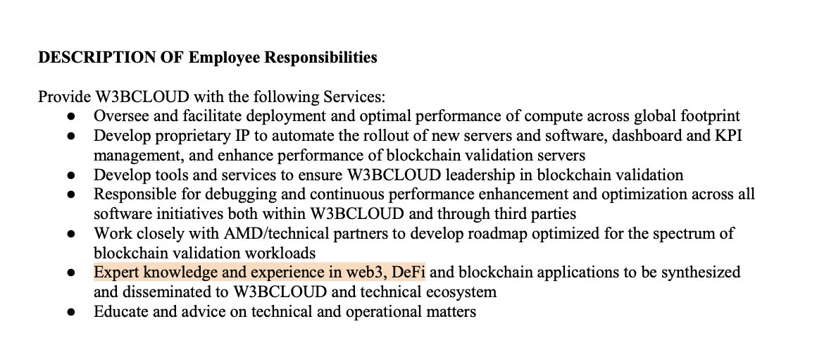
U.S. Securities and Exchange Commission@SECGov
The American values of economic liberty, private property rights, and innovation are in the DNA of the DeFi, or Decentralized Finance, movement.
English

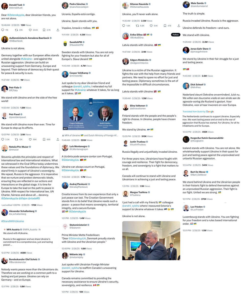
全世界都在支持泽连斯基英勇在白宫椭圆办公室抗争特朗普霸凌。
错了❌其实,一切都是精准的政治博弈和计算。
他其实只需要穿上西装、打上领带、面带微笑,感谢美国的支持,最后坐下来吃顿午饭,就能拿到一份体面的和平协议。
但凡看过全程视频都会问:泽连斯基的战术核爆:他为什么要主动炸掉谈判?
乌克兰正在输掉战争,这是冷冰冰的现实。
1.俄罗斯的战争机器开足马力
•在中国的工业支持下,俄罗斯每天能生产数千架无人机,每月发动上万次攻击,乌克兰根本拦不住。
•俄罗斯不在乎人命,朝鲜源源不断提供炮灰,他们能无限消耗,而乌克兰玩不起这个游戏。
2.三条路,只有一条能结束战争
•选项1:美国不仅送武器,还要送人,那意味着可能爆发第三次世界大战。
•选项2:乌克兰直接投降,普京彻底吞下乌东和克里米亚。
•选项3:接受特朗普提供的和平协议,进行妥协,至少还能拿回部分领土,这是当前唯一的现实选项。
问题来了:泽连斯基为什么要激化矛盾,把谈判彻底搞砸?
他其实只需要穿上西装、打上领带、面带微笑,感谢美国的支持,最后坐下来吃顿午饭,就能拿到一份体面的和平协议。结果呢?他选择在全球直播下挑衅特朗普、嘲讽范斯、不断激化矛盾,硬生生把谈判闹崩。
这不是冲动,而是战术核爆级别的自爆。
•战时总统不能成为“签妥协协议的人”
如果他签了停火协议,国内强硬派会视他为“叛国者”,他的政治生涯瞬间结束。
•他要把自己塑造成“抗争到底的烈士”
炸掉谈判,他就能继续站在“为乌克兰战斗到底”的道德高地,所有后果都甩给继任者。
•逼欧洲继续输血援助,拖延谈判
只要战争没结束,西方就必须继续给钱、给武器,他还能靠国际支持维持乌克兰的战时状态。
泽连斯基没有失控,他是精准计算后选择了断尾求生。
谈判破裂,他成了民族英雄,继任者才是那个签妥协协议的“替罪羊”。他赌的不是战场胜利,而是如何把政治遗产留到最后。
中文
让一个被自己挤走的创始伙伴回头把自己那么低价格收购了,这个行为跟众目睽睽之下切腹有什么区别
Polymarket Intel@PolymarketIntel
#BREAKING: ELON MUSK-LED GROUP OFFERS $97.4 BILLION TO TAKE OVER OPENAI - WSJ
中文
English

alma和我一样观点但人家明显专业多了。。。
Alma.Trk@alma271828
Lets analyse #opex + sentiment... Current economy datas (PPI and CPI) were softs, still haven't convinced market participants about this disinflationary trend to be sustained. Yields remain elevatedd due to term-premium as market expects sticky inflation and further stimulus under DJ Trump. What we see for now is a solely short covering and supportive vanna/charm flow in the $SPX, plus some fomo buying into the rally, but not a sentiment shift. Vol controls also add exposures on #volatility declines... ☝️Market reacted only on the fact that #Fed doesn't need to turn hawkish immediately, and #market has somse room to run up, but they also know that the fundamental underlying reasons behind the #inflation aren't gone and this rally is not sustainable, there will be a point were the #fed will need more room to sustain growth under agressive Trump policy and so market needs to go down... hedges are there into Q1 #opex... as written below in the quoted post... I explained this here, must read: x.com/alma18499/stat… ☝️ Market is pricing a 0 or 2 cuts for this year, bets a bit higher on 0 cut and one hike into EOY. ☝️If you understand what I wrote in the linked post, you can see that #Fed must be very slow. Bcs if inflation goes out of control, and #Fed becomes forced to hike, that can lead into a deflationary spiral at the end, and that would be a disaster. Many feels like that the aggressive inflationary Trump policy will lead into that scenario🚩 Today PM expo... So we have AM and PM expos. The AM expiring position effects you could see yesterday on those downsticks from an MM long iron condor at 5900/5910/5995/6000 $SPX with positive speed convexity inbetween. Now on the picture below you can see the PM expo for today. We have a MM net long speed environment below the marked zero speed line 6058.74 $SPX (My trendline of my reversion model is trending at 6046.24 $SPX This is a crucial pivot for the momentum on the wider timeframe) Long speed means that MMs net long upside gamma and net short downside gamma. (from dealer flow and vol perspective it doesn't really matter if upside gamma is ITM put or OTM call, or downside gamma is ITM call or OTM put bcs they are on the same side of the skew, and have the same vanna and charm profile) If MMs long OTM call gamma, they also long their vega and short their theta. And if MMs short OTM put gamma, they also short their vega and long their theta. Bcs skew is 25d put IV minus 25d call IV, what we have basically is a short skew position from MMs, and long skew from customers. Meaning, customers are net synthetical short stock, bcs they long OTM put and short OTM call that has the equvivalent P&L profile like a short stock position. This is a hedging position covering long stocks. Selling OTM call premium cover the purchase of the OTM put leg, and so long stock positions are hedged against a decline. This hedging position expires today. The MM long OTM call leg has long vanna and short charm values. So is the short OTM put leg also has long vanna and short charm values (bcs long OTM put has negative vanna and positive charm, but here MMs are short them, so the curves are inverted, multiplied by -1) This provides a net long vanna, short charm exposure for market makers. Remember, MMs have negative theta convexity☝️ So long vanna = vol up/delta up - vol down/delta down (positive relationship), and short charm means that as time passes MMs delta exposure decreases, making them shorter delta, that must be hedged by buying one delta assets. This is what we call delta decay, and what @jam_croissant refers to as "supportive vanna and charm flows". Long vanna however also means that vega convexity is positive (bcs vanna is vega convexity). Remember, MMs are long speed, so longer gamma to the upside and shorter gamma to the downside, but so is vega. So they long upside vega and short downside vega. Means, whenever the price moves up, they become longer vega that needs to be hedged by selling vol, that naturally supplies the market with more long gamma too. And vega also decays as time passes on the tails just like gamma. But as gamma increases vega decreases. But on expo days it is gamma, vanna and charm that matters. Lets see what does it tell for today... #intradaytrading We have a significant long gamma strike at 5952 $SPX This is the middle of an MM long butterfly spread of 5990/5952/5875 $SPX (See: x.com/alma18499/stat… ) This means magnetic effect towards this strike as long as $SPX can break and hold above 5975.48 $SPX (only 3 pts above my coded risk lvl) If this lvl breaks, momentum can climb up towards more higher/stronger gamma strikes at 6030 $SPX I code 5860 $SPX as the zero vanna, also coincidencing the cluster of the nearest customer long put positions, that will expire worthless and provide supportive MM buyback flow as their delta decay accelerates. We can expect a retest of my trendline written above. However into the next week these supportive MM buyback flows will be gone and that will be the time when customer sentiment will reveal itself. Note that gamma (if charm convexity is positive) increases towards the expo. And also that gamma and vega have inverse correlation as I pointed it out here: x.com/alma18499/stat… Also means that when the expo is gone, #volatility will have an impact. So what I want to see is that customers remain short skew, in order to stuff MMs with long gamma. Reversion points and risk lvls are attached for $SPX and $ES $ES_F long bias maintains🟢 Hope you liked it: buymeacoffee.com/alma18499 #optionstrading #stockmarket #riskmanagement
中文
@garyblack00 This is Apple versus android story. Tesla will make 95 percent of profit, everybody else fighting for the life over 5%
English
$TSLA -4.2% today after BofA analyst John Murphy downgraded TSLA to Hold from Buy, noting investor sentiment has "shifted more positively" and "catalysts around future growth drivers have been more fully recognized," including the potential for self-driving robotaxis. Some also attribute TSLA weakness today to comments at CES by NVDA CEO Jensen Huang that NVDA is working with nearly every automaker to develop their autonomous driving capabilities, although that was likely already well known.
English
Charlie H. retweetledi

Charlie H. retweetledi
🚨 $KIP IS NOW LIVE! 🚨
Official $KIP (ERC-20) Contract Address:
0x946fb08103b400d1c79e07acCCDEf5cfd26cd374
Trading available on:
✅ @kucoincom
✅ @gate_io
✅ @BingXOfficial
✅ @Uniswap
⚠️ Do not interact with unofficial contracts. Stay vigilant to avoid scams.
English
Charlie H. retweetledi

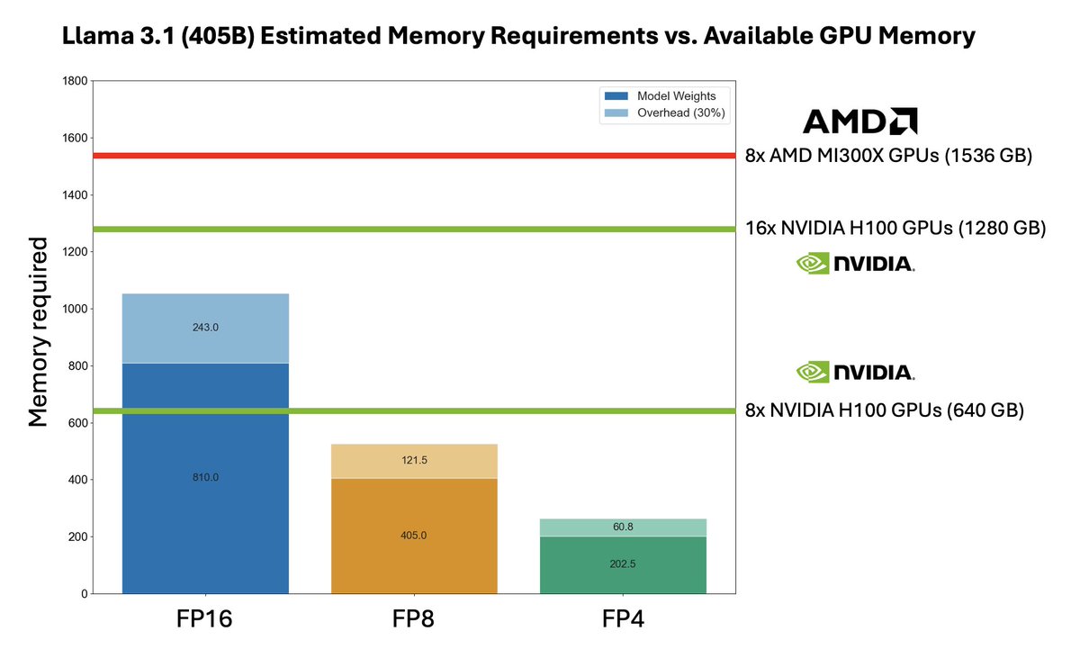
Llama 3.1 405B could be the catalyst for much greater #AMD adoption for AI inference 📈
@AMD's MI300X may be uniquely suited to cost-effective Llama 3.1 405B inference. Its 192GB of memory allows a single 8xMI300X node to serve Llama 3.1 405B in its native FP16 precision - whereas two 8xH100 nodes are required on @nvidia.
As we have previously covered, a single NVIDIA 8xH100 node only has 640GB of memory - not enough to hold Llama 3.1 405B’s full 810GB of FP16 weights in memory at once. This means that providers are forced to deploy two 8xH100 nodes with interconnect to serve 405B in FP16 precision, forcing them to accept a significant cost and complexity penalty.
Nvidia’s future H200 and B100 come with 141GB and 192GB of high bandwidth memory respectively - but unlike those, AMD MI300X is available now. @LisaSu noted on AMD’s Q2 earnings call that AMD was demand-limited on MI300X for the remainder of 2024. Will Llama 3.1 405B alone flip that narrative?
We are starting to see adoption and support increase. Both @FireworksAI_HQ and @LeptonAI are hosting Llama 3.1 405B on AMD MI300X chips. They stand out as the lowest cost providers of Llama 3.1 405B. However, it is important to note they are serving the model at FP8 and INT8 precision respectively.
Furthermore, projects like GPU.cpp from @answerdotai (@jeremyphoward, @austinvhuang) are making it easier than ever to write and run portable code across different chip (hardware & software) architectures - decreasing the CUDA lock-in.
What is your view? Long #AMD?
English


Charlie H. retweetledi

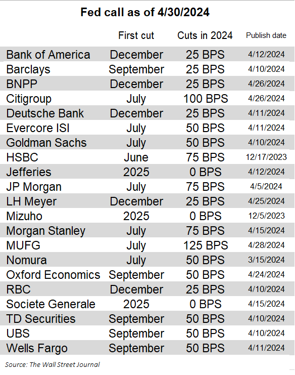
Fedwatchers continue to push back their expectations of when the central bank will lower rates
More of them now anticipate just one or two cuts this year—and that was before Tuesday's uncomfortable ECI report wsj.com/livecoverage/f…
Nick Timiraos@NickTimiraos
The March inflation report triggered a jailbreak by the sell-side bank and other Fed forecasters, who largely abandoned prior calls for a June cut Most now see the first cut no sooner than Q3, and there's been a lot of movement towards expecting just one or two cuts this year.
English