
Harm Knoops
296 posts
Harm Knoops
@HarmKnoops
Atomic Scale Segment Specialist at Oxford Instruments and Part-time Assistant Professor at Eindhoven University of Technology
Eindhoven, The Netherlands Katılım Haziran 2011
175 Takip Edilen330 Takipçiler

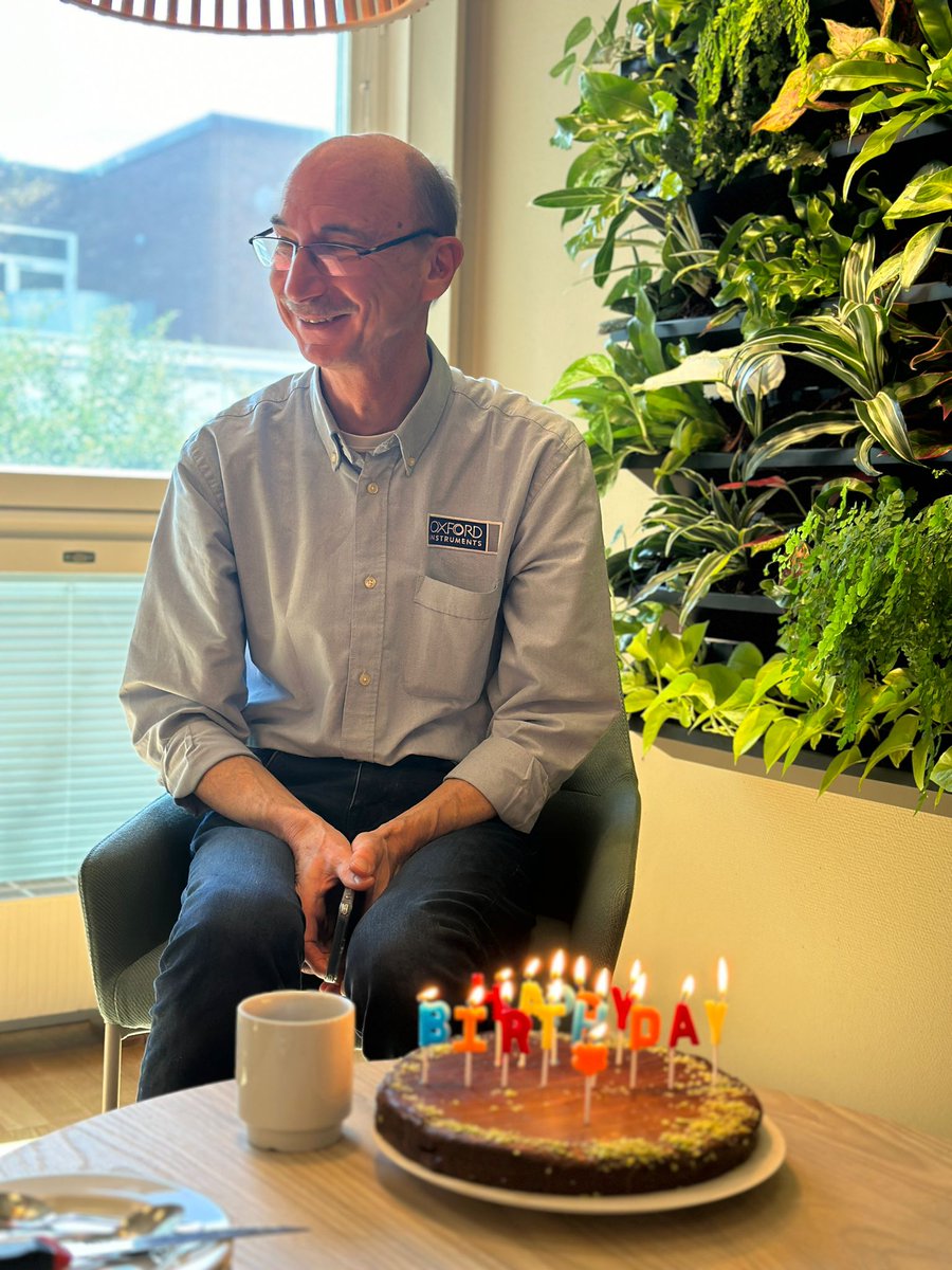
The birthday boy made it - plasma is on with a brand new PLC at @AlixLabs in Lund @OxInst @HarmKnoops #aletch

English
Amazing devotion to customers is celebrated at @AlixLabs today, when Ralf Fuerst from @OxInst Instruments plc Upgrades the PLC on our Original Oxford Plasma Lab 100 ICP and we celebrate his 66 year birthday! #Plasma #plasmaetch #ALEtch
English
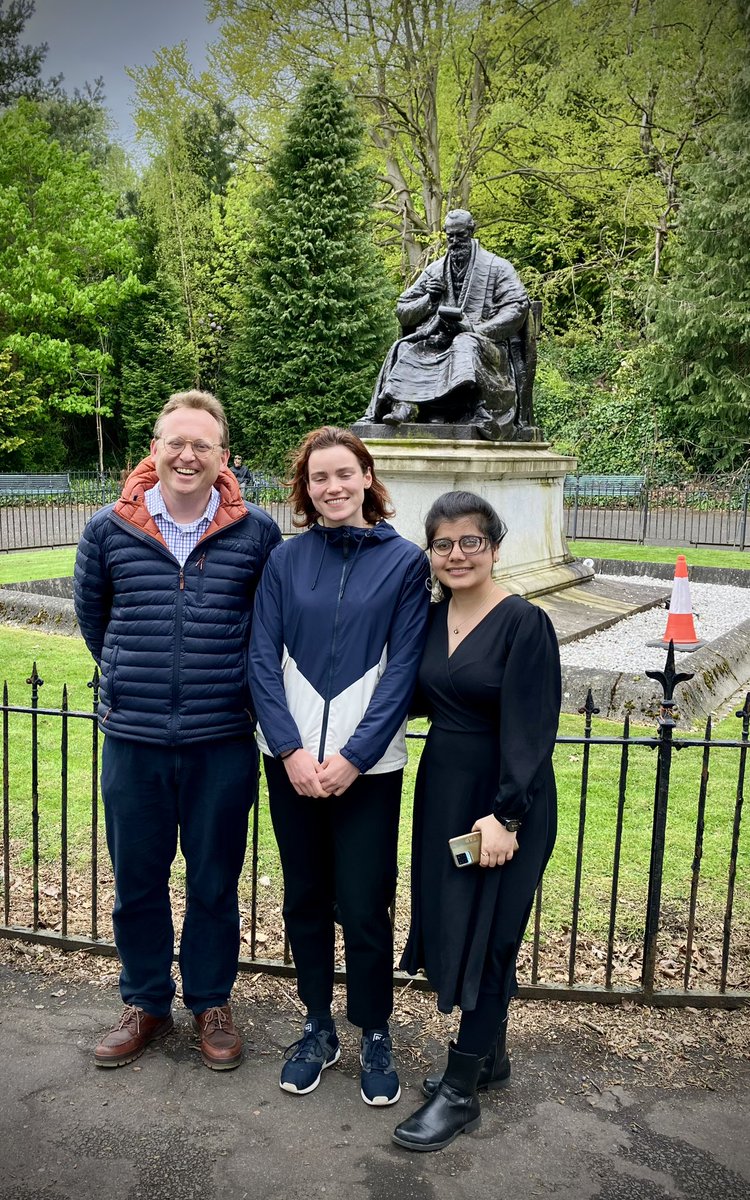
@QuantumSensors @TUeindhoven @UofGlasgow @UofGEngineering @UofG_JWNC @UofGARC @ErwinKessels In-person visits bring extra strength and depth to collaborations so thanks again for making this possible. And looks like you're also showing some of the nice Glasgow scenery 😊.
English
Very pleased to host Silke Peeters @TUeindhoven 🇳🇱 this week @UofGlasgow @UofGEngineering @UofG_JWNC @UofGARC Strengthening our partnership on #ALDep for #quantum tech 🏴 🤝 🇳🇱 @ErwinKessels @HarmKnoops
English
Cheers - @OxInst lands major Japanese orders for advanced GaN #ALEtch and #ALDep systems, boosting power electronics and 5G/6G device production
@HarmKnoops #galliumnitride #Japan blog.baldengineering.com/2023/11/oxford…

English
@jv3sund Bias-Voltage ALD 😄, not sure what the i would stand for in this case
English

Proud of Silke Peeters for the first paper in our project @TUeindhoven. Plasma #ALDep of high-quality TaCxNx-1 using substrate bias, these ultrathin superconducting films are promising for a range of #quantum devices.@OxInst @QuantumSensors @ErwinKessels doi.org/10.1063/5.0169…

English
At @euroCVD #BalticALD, Silke Peeters @TUeindhoven discusses how substrate biasing can help plasma #ALDep of tantalum carbonitride for quantum devices

English
@jv3sund @aldjournal I would've thought by now you would have organized an ALD event there 😄
English
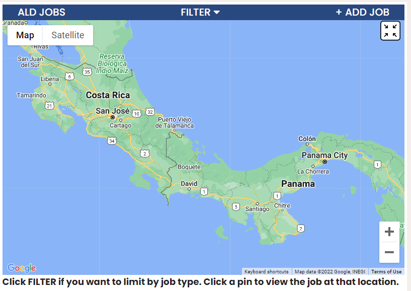

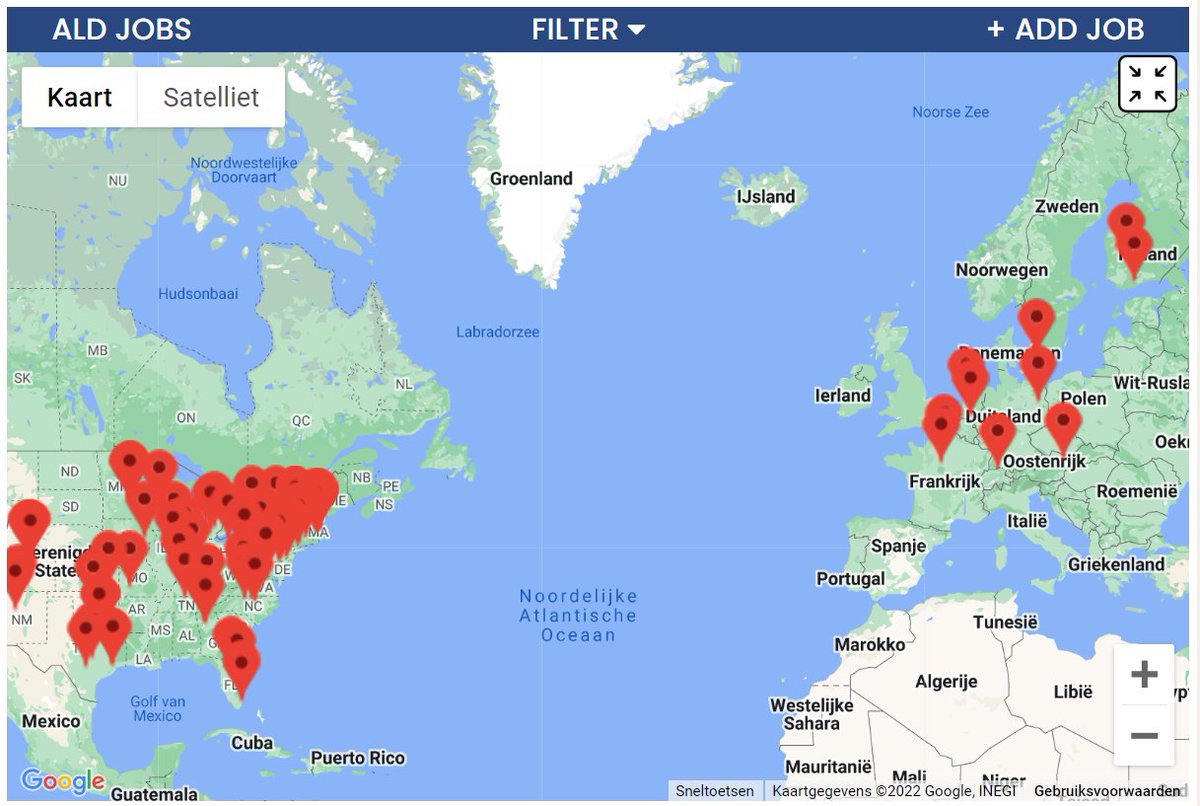
Did you know that you can find a global job map on atomiclayerdeposition.com? Find and place job opportunities related to ALD, both academic and industrial. Take a look today and share: bit.ly/3HORyjA #ALDep #jobs #materialscience #chemistry
English
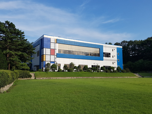
@ErwinKessels @jv3sund Maybe I can convince Oxford Instruments to add a few colors to their new building. The blue square is already there :) oxinst.com/news/oxford-in…
English
Cool presentation yesterday at #AVS68 by Haozhe Wang from the Minnich group @CalTech on isotropic #ALEtch of AlN done on an @OxInst FlexAL. Great to see that the SF6/TMA process pioneered by Nick Chittock @TUeindhoven has many applications.

English
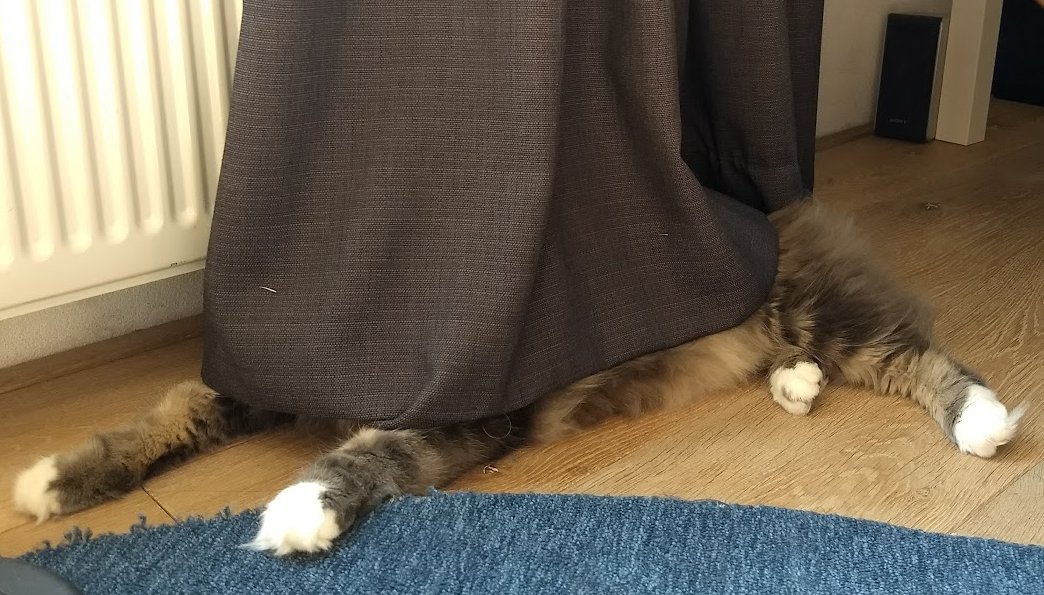
@eray_aydil This is our cat Nano, he also says hi. Since Nano is only a small Siberian cat he can be difficult to see by the naked eye.
English

"Why NIST Is Putting Its CHIPS Into U.S. Manufacturing"Nice flexing background! @HarmKnoops #ALDep LINK: nist.gov/blogs/taking-m…

English
@ErwinKessels @TUeindhoven I'll try not to be traveling for the next picture 😄.
English
The Plasma & Materials Processing group @TUeindhoven has a new group photo! Unfortunately some people are missing... But what a great group of people! So happy to work with them!

English
@jv3sund @DrFrederickChen @TUeindhoven @ErwinKessels Note this work is from the Elementary Processes in Gas Discharges group. So although it is @TUeindhoven
it is from @gkroesen and @SanderNijdam
English
@DrFrederickChen So much of the semiconductor-relevant Plasma work is done at @TUeindhoven. @ErwinKessels
English

EUV-induced hydrogen plasmas caught attention briefly but some characteristics still not clarified, like the emission at longer EUV and VUV wavelengths (20-100 nm). These can still expose the resist at close proximity.
One starting reference: lnkd.in/ddmXRfRc
English
@jv3sund @ErwinKessels As for most process results each might have a different useful application. Both cheeses can be good 😄.
English
While being ASM ALD Tool owner for 10 years I got a Dutch Cheese every Christmas - here now Swiss vs. Dutch #ALDep Cheese @HarmKnoops @ErwinKessels
Paper: pubs.acs.org/doi/abs/10.102…
English
@ErwinKessels @TUeindhoven Excited about this upcoming project and working with all the partners @TUeindhoven, @OxInst, @UofGEngineering, @quant_ware, @orangeqs and Kavli Delft. Silke hit the ground running with her first conference presentation on plasma #ALDep of superconducting TaCxNy at #ALDALE2022.
English
#ALDep and #ALEtch have "saved" the semiconductor industry but both atomic scale processing methods are also expected to become key fabrication methods for Quantum Technology devices. Here you can read more about our new project @tueindhoven. @HarmKnoops atomiclimits.com/2022/07/20/ald…
English
English
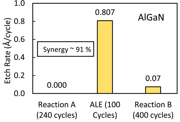
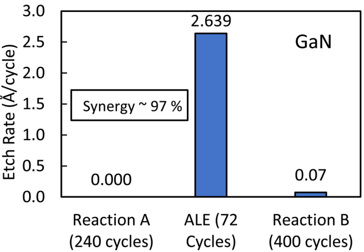
Using our system 𝗣𝗹𝗮𝘀𝗺𝗮𝗣𝗿𝗼 𝟭𝟬𝟬 𝗖𝗼𝗯𝗿𝗮, the @UofGlasgow showed a high synergy (>𝟵𝟭%) #ALE process. Such #etching is essential in enabling high-performance enhancement-mode #GaN field effect devices. Read more:
okt.to/oxsPE5+
English
@JVSTAB @AVS_Members Nice collaboration between @imec_int and @OxInst on low-damage plasma #ALEtch of dielectrics on top of #2Dmaterials using controlled Cl2–BCl3 doses and Ar ion enhancement
English

ICYMI: Plasma Enhanced Atomic Layer Etching of High-k Layers on WS2 #JVSTA @AVS_Members avs.scitation.org/doi/10.1116/6.…

English