
Sabitlenmiş Tweet
acceler8future
50.3K posts

acceler8future
@acceler8future
Elon, Tesla, $TSLA and 🚀 future Replies - Conservatives, Arsenal and more
Somewhere near London Katılım Şubat 2024
1.6K Takip Edilen3.3K Takipçiler


When Elon Musk challenged Mark Zuckerberg to a cage match, Musk cited his \(300\)lb weight advantage and larger size as his primary edge. He famously stated: "If the fight is short, I probably win. If long, he may win on endurance. I am much bigger and there is a reason MMA has weight divisions."
Happy Punch@HappyPunch
Sumo wrestler destroyed a 5-0 pro boxer in an MMA fight last night 😳
English

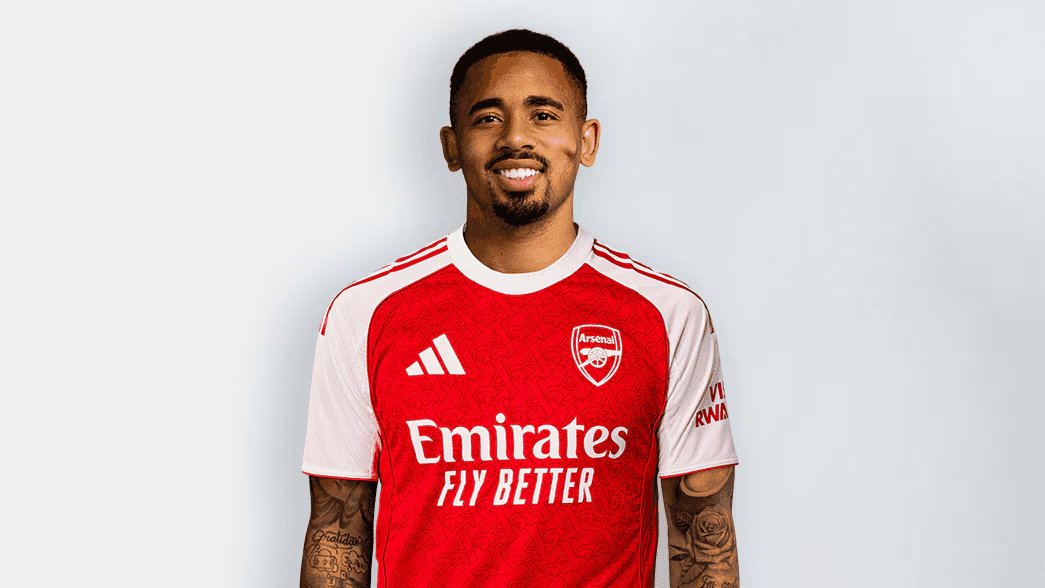
Give Gabriel Jesus 1 more year at Arsenal
Yes or NO?
English
acceler8future retweetledi

Grok foundation model V9-Medium (1.5T) has finished training. Evals look good. A lot of Cursor data was added in supplementary training and there is more to come.
Fine-tuning is underway and reinforcement learning begins in a few days. 2 to 3 weeks to public release.
This will be a major improvement over the 0.5T v8-small that currently serves all Grok production traffic, especially for difficult coding tasks.
English

A male bee mates for less than 5 seconds in midair. The ejaculation is so explosive you can hear it pop from a few feet away. His body rips in half. He falls dead before hitting the ground. And he is one of the lucky males in the hive.
When a male bee, called a drone, chases down a queen mid-flight at speeds of 22 miles per hour, his entire reproductive organ turns inside out. The pressure required for this comes from nearly all the blood in his body, which rushes downward to force the organ outward like a spring. The semen fires into the queen with so much force it makes the audible pop. The organ then snaps off and stays lodged inside her like a cork. As he flips backward off her body, his abdomen rips open. The next drone waiting his turn has to physically yank out the dead male's cork before he can mate. The same thing then happens to him.
The queen does this 12 to 20 times in a single afternoon. She flies up to a spot in the sky that beekeepers call a drone congregation area. Picture an invisible meeting point about 50 to 130 feet above the ground where up to 11,000 male bees from as many as 240 different hives are hovering, waiting for her. These spots stay in the exact same locations year after year, sometimes for over a decade. No one fully understands how brand new drones, born only weeks earlier, find them.
By the end of her mating run, the queen has collected around 100 million sperm cells. She keeps only 5 to 6 million in a tiny internal storage organ that keeps them alive for years. From that supply, she uses just two sperm cells per egg for the rest of her life, laying up to 2,000 eggs a day for 2 to 7 years. After that one afternoon in the sky, she will never mate again.
A 2019 study from UC Riverside, the University of Copenhagen, and the University of Western Australia found that bee semen contains toxic proteins that temporarily blind the queen by interfering with how vision genes function in her brain. If she can't see well, she can't fly out again to mate with more males. Their semen also carries a separate protein that attacks and kills sperm cells from rival drones still inside her. The males keep competing long after every one of them is dead.
The 99.9% of drones who never get to mate have it worse. As autumn arrives, the female worker bees in the hive stop feeding their brothers, then drag them out of the entrance after biting off their wings. The drones can't fly back in. They starve or freeze in the grass within days. The colony raises a fresh batch of disposable males the next spring, and the whole cycle starts over.
𝙍𝙞𝙘𝙠 🥊@RickCombatTV
Male bee dies after ejaculation while mating with a queen bee
English
Silver still looks like the future
Sawyer Merritt@SawyerMerritt
I'm having a hard time finding a color the Cybercab doesn't look good in.
English
Number 1 priority is to buy $SATS with 40% upside vs $SPCX IPO price
Number 2 is a cheeky bet on $ASTS
Number 3 is don’t sell your $TSLA
Number 4 is buy $SPCX if you can but only if you are prepared to wait. $TSLA shareholders will understand.
Leo Edge@LeoCapital_01
A message for my $TSLA friends eyeing the SpaceX IPO $SPCX. I traded $TSLA for years. I know the community. I know the excitement when Elon takes something public. But before you chase @SpaceX at $1.75 trillion, read the S-1 carefully. SpaceX doesn't need your money. They raised at $800B in private tenders six months ago. They could raise $50B privately tomorrow with a phone call. This IPO isn't about raising capital. It's about giving insiders liquidity. 95% of @SpaceX shares are held by insiders. Only 5% will be publicly traded. Insiders hold $1.66 trillion in paper wealth they currently can't sell. The IPO changes that. And they've structured it so insiders can sell BEFORE the standard 180-day lock-up expires. @SpaceX built in early release provisions -- after the first earnings report, insiders can sell up to 20% of their shares. They're also reserving 30% of IPO shares for retail. Ask yourself -- when has Wall Street ever given retail the best seats in the house unless retail was the product? 100x revenue. $4.9B net loss. xAI burning $6.4B a year while @Starlink subsidizes it. This isn't 2020 Tesla at 20x revenue with a clear path to profitability. This is a different risk profile. Now here's the part I want you to actually consider. SpaceX's S-1 sizes their satellite-to-phone business (Starlink Mobile) at a $740 billion TAM. Their Connectivity segment does $11.4B at 63% EBITDA margins. Those numbers are real and impressive. But buried in the S-1, @SpaceX names their D2D competitor: $ASTS . @AST_SpaceMobile $40 billion market cap. Not $1.75 trillion. $40 billion. Here's what $40B buys you: 98.9 Mbps proven from space to unmodified phones (SpaceX does 3-5 Mbps) The only low-band D2D spectrum access on Earth (indoor coverage SpaceX can't match) All three US carriers forming a joint venture around ASTS technology Google invested $358M their largest public equity holding AT&T, Verizon, Vodafone as equity investors $3.5B cash, $1.2B contracted backlog 3,900 patents, custom ASIC in production Three satellites launching on a Falcon 9 next month 60 carrier partners covering 3 billion subscribers @SpaceX at $1.75T is pricing perfection across rockets, satellites, AI, and Mars. One miss and it corrects hard. $ASTS at $40B is pricing uncertainty in a $740B market where the technology is already proven and the carriers have already chosen sides. The Tesla community knows what it feels like to find a mispriced stock before the world catches on. $TSLA at $30 pre-split wasn't obvious to anyone except the people who did the work. $ASTS at $106 in a $740B market with 33x faster speeds than SpaceX D2D, a carrier JV, and institutional discovery just beginning -- that's the same kind of setup. So before you throw money at a $1.75T IPO where insiders are building exit ramps, maybe look at the $40B competitor they named in their own filing. Not financial advice. Just math. $ASTS 🛰️ cc @SawyerMerritt @unusual_whales @DanBTC916
English
@KawzInvests $SATS is a $SPCX proxy who have X Money. All I need on the FinX side of things.
English

Football has Pelé. Maradona. Ronaldo. Messi.
FinX has its own GOATs.
Who are your 4?

English

Regulations don’t always make the world a better place
Or
Regulations nearly always make the world a worse place?
Sawyer Merritt@SawyerMerritt
Lars Moravy in new interview on why the @Tesla Model S and Model X were discontinued: "Every 5 years or so Euro NCAP updates their protocols. Looking forward, they are getting more stringent. Some of the IIHS stuff. We want to make the safety cars on the road, and that means always making structural updates. We were at the point where this platform, like it was never designed for the small overlap and the offset cases that exist now on Europe NCAP and IIHS. We made bandaids along the way to make sure it was being safe in those positions, but it was just like man it's going to be a massive overhaul. At the same time, going back to the room it was like we were talking about Optimus and like where do we put Optimus and it was like well we got to spend you know however many hundreds of millions of dollars to redo this in this factory, but we also need a pilot factory for Optimus. And it just kind of was like serendipitous. I think that the two things went hand in hand. You said who was the first one to bring it up. The future is autonomous. These cars were the first ones we designed. They're the least ready for that, you know, world. So, we got to move forward." Sounds like it just wasn't worth the investment, since it was likely going to cost several hundreds of millions to retool and redesign, and maybe even more to build a pilot Optimus factory somewhere else, when it would just make more sense to use the S/X space in the Fremont factory. (You can listen to the full interview in Ryan’s post below)
English
@PepInvestStocks This might mean $SIVE are first to embrace LPKF glass interposers. Although I'm expecting $KOPN microLEDs to dominate.
English

$SIVE (Fabless) vs. $LITE (Vertical Integration)
Sivers shares the market with two of the world’s most powerful manufacturing giants. The division of roles is perfectly optimized:
$SIVE (The “Intellectual Power”): ~124 employees develop the proprietary, architecturally unique laser design and own the IP.
WIN Semiconductors (The Wafer Fab): ~3,000 employees operate the cleanrooms and turn the design into Indium Phosphide (InP) wafers.
$JBL (The Packaging Giant): ~140,000 employees integrate the lasers into final products such as optical engines, ELS modules, and transceivers.
The key point: Sivers does not have to directly employ or pay a single one of these ~143,000 partner employees. Sivers simply purchases wafer capacity and sells the finished high-margin product (the laser or licensed design) to CPO customers.
$LITE: ~10,500 employees
Lumentum follows the traditional vertically integrated model. They own their fabs, their packaging facilities, and must manage a global organization of more than 10,000 employees.
That means: enormous fixed costs, heavy depreciation from factories and equipment, and significant exposure to cyclical market downturns.
The Massive Leverage for $SIVE
Once the volume ramp begins around 2027, this structure creates two extremely powerful effects that generalist analysts completely miss in their models.
1. Infinite Scalability Without Capital Expenditures (CapEx)
If a CPO customer such as Ayar Labs or a hyperscaler increases orders from 10,000 to 10 million laser arrays per year, the following happens:
$LITE may need to build additional fabs, expand cleanrooms, and hire hundreds of new employees. This pressures margins in the short to medium term.
$SIVE simply calls WIN Semi and Jabil. Because these giants already scale for the global tech industry, they can absorb the volume shock with ease.
Sivers itself would not need to add a single employee.
Revenue could increase by 100x while fixed costs tied to its ~124 employees remain nearly unchanged.
2. Astronomical Revenue per Employee
This is the metric that drives technology multiples on Wall Street and the Nasdaq.
At Lumentum, revenue is spread across a massive workforce of more than 10,000 employees.
At Sivers, the revenue from a large-scale volume ramp flows through an organization of only ~124 people.
Once commercial contracts begin scaling, Sivers’ revenue per employee could surpass Lumentum’s, and that of most semiconductor companies, by a wide margin.
This is precisely the metric that allows software companies to command premium valuations.
Sivers is effectively replicating a software-like margin structure within the hardware sector.
$LITE may be larger today, but it carries the inefficiencies of a giant organization.
$SIVE by contrast, leverages WIN Semi and $JBL to harness the manufacturing power of approximately 143,000 workers while remaining lean, agile, and potentially highly profitable.
Anyone valuing Sivers using traditional semiconductor frameworks may fail to understand this asymmetric leverage.
Serenity@aleabitoreddit
Photonics is nuanced and using ChatGPT/Gemini makes you miss all of it: 1. $SIVE is actually a chokepoint and partially a bottleneck. The reason it's a chokepoint is leading CPO/optical hyperscaler players go through Sivers, likely: Ayar. Celestial. Lightmatter. Lightelligence. Poet. If you take out Sivers, you literally can't make some of their products + delay their roadmap by years. As many are sole/primary source but are heading the direction on multi-source. As for the bottleneck argument: Win Semi is the bottleneck for scaling laser production. But... the nuance is when you have capacity allocated for the next few years. You become part of the bottleneck itself if players fight you for allocation of finished lasers. That's the nuance people miss with capacity allocation dynamics. It's like saying $SNDK is not part of the NAND bottleneck when Kioxia makes all of it. But when Sandisk has the ultimate control of output supply, they become the bottleneck + have all the pricing power. Sivers controls output supply of CW lasers given allocations, and as seen with $LITE earnings, CW laser is currently bottlenecked as everyone seems to be stuck producing EMLs. 2. Like how LLMs always uses em-dashes. You can tell when people use AI when they always use the same "CW is a dumb interchangeable laser" argument or compare "power" specs after conflating different architectures. That's why your "analysts" using AI will get this wrong over and over. There's CW lasers... and then there's a specific architectural design that Sivers achieves with DFB lasers. If you compare power specs with $LITE vs. Sivers, Lumentum wins in isolation. But they're completely different laser architectures. All the leading CPO players like Ayar, chose $SIVE for an architectural reason for high power, low thermal, laser arrays. $JBL 1.6T LRO also made one of the most dramatic moats cited by their fireside chat, using Sivers lasers. If you think CW lasers are interchangeable with Sumitomo/Furukawa, and others. And can be plug-and-play... i don't know what to tell you? Again: $SIVE makes architecturally unique CW lasers for leading CPO players. 3. I'm not sure how many times I need to say this: $SIVE for 2024-2025 has been going through development contracts. People using TTM revenue or former P/S metrics are using completely the wrong metrics, when there's volume ramp in 2027. It's the same with $AAOI which volume ramps in H1 2027. $AEHR which volume ramps after qualification. $LPK that volume ramps after qualification. This is just missing qualification cycles in semiconductors and how to model financials currently. As for the $LITE comparisons (which was also my long last year): $LITE literally started off selling laser dies before acquisition of Cloud Lite and other downstream optical engine components. This is where $SIVE is at today with starting off in the laser chokepoint for CPO: People are modeling laser revenue off very isolated TAM projections. Meanwhile Sivers is targeting M&A to expand revenue for TAM projections. This is not a simple component FAU + ramp valuation modeling over with a Taiwanese company. Since Laser companies like $LITE, $COHR are known to downstream expand to make their lasers more valuable, then vertically integrate (fabs, assembly) afterward. Again, Sivers worked with Ayar and these types of companies before they all became billion dollar companies. I have high conviction knowing they know what to acquire down the ELS/optical engine stack + pluggable transceiver for TAM expansion. It's just annoying when I get people who don't understand the nuances backseat commenting wrong things about my longs. I got the same thing about $AXTI is not a bottleneck! InP isn't needed! China! back at $14. Now it's $140 I got the same thing about $AAOI "is going down 50%!" back at $65. or "AOI management is shady at $30". Now it's $170 I got the "there's nothing new with $SOI" back at $45. Now it's $170. I think I'm one of the few who actually understands the nuances with photonics, since I did call out $LITE, $TSEM, Innolight, $AXTI, $AAOI, $SOI, that outperformed both photonics markets and overall markets over the past year. And now I'm long on $SIVE.
English
@DMC_Ryan @larsmoravy @woodhaus2 Tesla Roadster will be made in Austin. @grok what else was said about Roadster?
youtube.com/watch?v=Ej8rIS…
YouTube
English
Tesla friends: my new interview with @larsmoravy & @woodhaus2 is here! It's all about the history & legacy of the Model S & X. The guys tell some really awesome stories from over the years (& give us a nugget of new Roadster news too). Timecodes and MP3 link below. Enjoy!
00:12:18 Interview Start
00:13:30 How the Decision to Discontinue S and X Happened
00:18:02 S and X Would Need a Complete Redesign to Continue
00:21:55 Next-Gen Roadster News
00:25:03 Signature Numbers
00:29:03 Final S and X Production Numbers
00:29:43 The Beginning of Model S
00:36:20 More Lightning
00:36:48 Old S and X Stories
00:39:26 First Drive of the Model S...Ever
00:45:14 The EV Market and EV Adoption Rate
00:49:36 Adding Dual Motors to Model S
00:51:36 A 3rd Motor in a Model 3?
00:54:37 About the Never-Made Model S Plaid+
00:56:58 Are 18650s done at Tesla?
00:58:10 Favorite Wheels
01:02:10 Pencils Down on S and X
01:03:22 Parting Message
01:05:07 Drive or Preserve their Signature S's
pscrb.fm/rss/p/traffic.…
English
acceler8future retweetledi

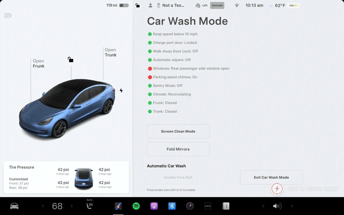
Tesla's Car Wash Mode is genuinely one of those features you didn't know you needed until you use it.
One tap and it closes windows, locks the charge port, disables auto wipers, turns off Sentry Mode, silences parking sensors, and gives you a live checklist of everything that could go wrong in an automatic car wash.
It even has a one-tap button to put the car in neutral for conveyor belt washes, which anyone who's fumbled with a Tesla gear stalk in a car wash line will appreciate.
Small feature that saves a lot of headaches.
Source: @tesla, Not A Tesla App
English

What was the most interesting Tesla / EV / AI news of the week?
English
@AFTVMedia Havertz needs to start the final with Gyokeres replacing him at 60 mins.
English


@Arsenal You may have forgotten.
Dowman is a match winner!
English

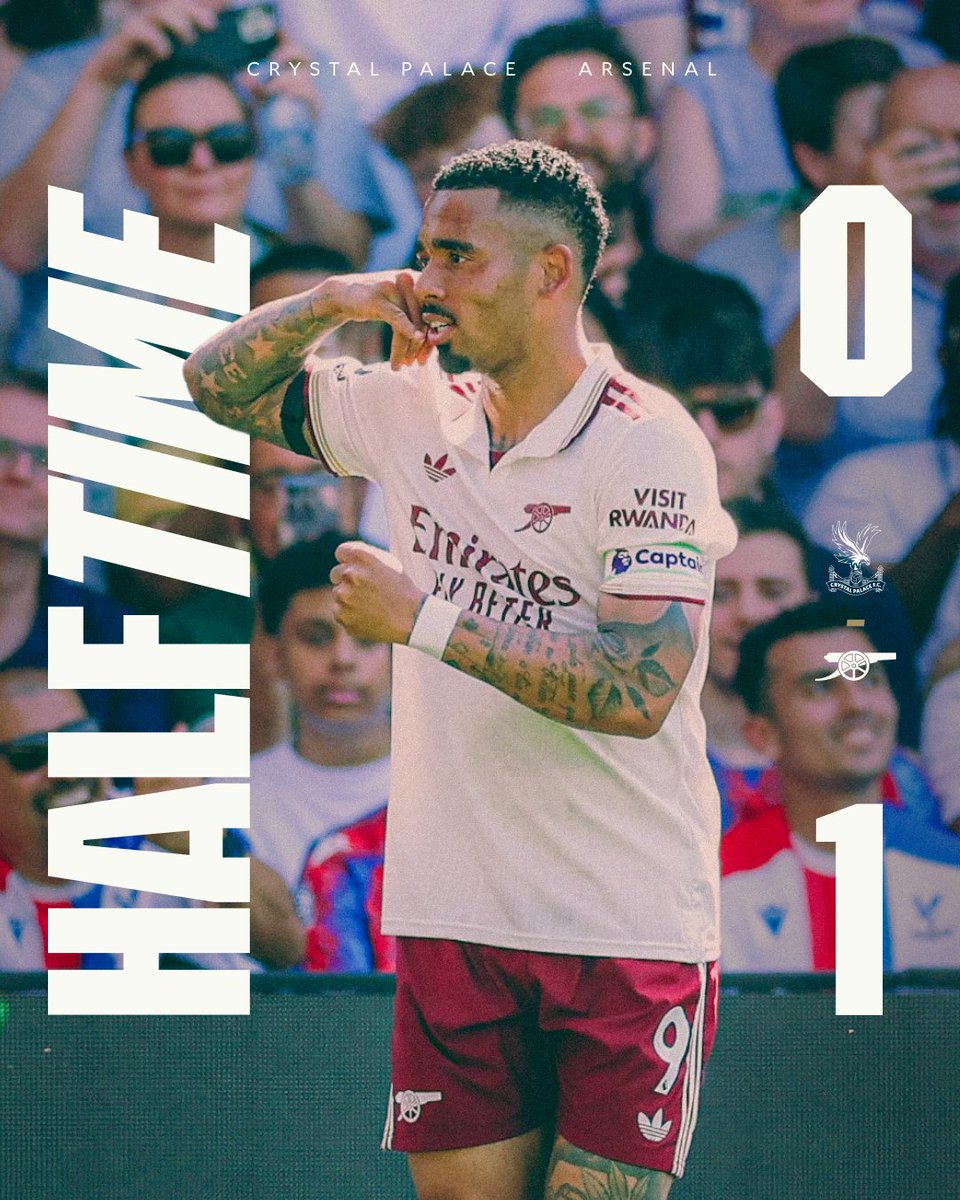
@AFTVMedia Two great opportunities wasted by Jesus. Martinelli had a tap in...
If we get £30 for him I would be amazed!
English

Actually, old bean, I’ll be in the USA for many of the World Cup matches. I will be cheering on Scotland, England, France and the USA.
If England plays France or USA I will cheer on England.
If France plays USA I will cheer on France.
Whoever Scotland plays I will be cheering on Scotland. Always.
I trust that clarifies my position. I know it troubles you a lot and that this full explanation will help you sleep better.
Thank you for your attention to this matter!
🏴DavoM🏴@Davo_Mack
@afneil Paisley born Andrew will be cheering on England at the World Cup from his French home, there’s a name for this kind of person 🤔
English