Amaan Rehman Shah
9 posts

Amaan Rehman Shah
@amaanssh
bug hunter @ etched
San Jose, CA Katılım Mayıs 2018
153 Takip Edilen19 Takipçiler

Took us a minute, but stacked PRs are now on GitHub 🥞
github.blog/changelog/2026…
English
A year here and I’d sign up again tomorrow
Etched@Etched
We’ve raised $300M in Series C funding at a $10.3B valuation from Sequoia, Andreessen Horowitz, Jane Street, Argo, and SK Hynix. Our mission is to run the world's inference. This round accelerates production of our inference clusters. We've opened an 80,000-sqft, 10-MW facility 15 minutes from our office to expedite production and prototyping.
English
@wafer_ai great breakdown. the real shift is inference getting first-class silicon instead of hand me downs from training. lots of different routes being taken right now. fun era to be building silicon that isn't a GPU.
English

🚨 OpenAI is launching GPT-5.6 Sol on Cerebras at up to 750 tps.
Here's How kernels work on Cerebras Chips
cerebras built a chip with 900,000 cores on a single silicon wafer.
CSL (Cerebras Software Language) is a Zig-inspired DSL that gives you direct control over the Wafer-Scale Engine. the SDK is publicly documented and the programming model is genuinely the most alien one we've ever looked at.
in CUDA you write one thread's perspective and launch millions. in CSL, there are no threads, no warps, no shared memory, and no kernel launches. you write code for individual Processing Elements: 900,000 independent cores arranged in a 2D mesh on a single silicon wafer. each PE has its own 48 KB of private SRAM, its own program counter, and a 5-port router connecting it to its 4 neighbors. that's actually it. no DRAM. no HBM. no cache hierarchy. 48 KB is your entire world per PE, where code and data must both fit.
the programming model is dataflow.
data moves between PEs as 32-bit messages called wavelets, traveling along virtual channels called colors. when a wavelet arrives at a PE on a specific color, it activates a task (a chunk of code bound to that color at compile time). tasks run to completion, then hardware picks the next activated task. tasks cannot call each other. they can only be activated.
so instead of "launch N threads," you think of it like: "place code on PEs, define routes, let data flow."
the memory model is also very different from GPUs.
on an H100 you get 80 GB of HBM shared across all SMs. on the WSE-3, memory is 48 KB per PE, and there are 900,000 of them! this gives you 44 GB total on-chip SRAM at 21 PB/s aggregate bandwidth (vs 3 TB/s on H100). every access is single-cycle. no coalescing needed. no bank conflicts. no cache misses. but also no way to access another PE's memory. all inter-PE communication is explicit wavelet routing through the fabric.
take a distributed GEMV for example. you would write a layout file that physically routes wavelets across the mesh. two PEs sit side by side. the left PE computes a partial result and routes it eastward. the right PE receives those wavelets from the west and accumulates. routing is defined at compile time. both operations are asynchronous and activate a task when they finish. you're physically routing data across silicon at 1 clock cycle per hop.
cerebras is an extremely technically interesting & alien beast. reports 95-210x speedups over H100 on stencil computations. 3,000 tokens/sec inference on gpt-oss-120B. $10B+ deal with OpenAI for 750 MW of inference infrastructure. very exciting times for alternative accelerators!
deep dive 1/6 by @gpuemi

English
@tomwarren We really went from the cloud back to a physical disc, full circle
English

I had to check it wasn’t April 1st 🤯
GitHub@github
We heard you. And we agree. In light of recent developments in physical media, GitHub is proud to announce that you can now obtain your public repo on CD-ROM. Keep it. Lend it to friends. Pass it on to your children. Your code is physically yours, forever. Until you lose it, let's be real. Order yours today. gh.io/cd
English
Amaan Rehman Shah retweetledi

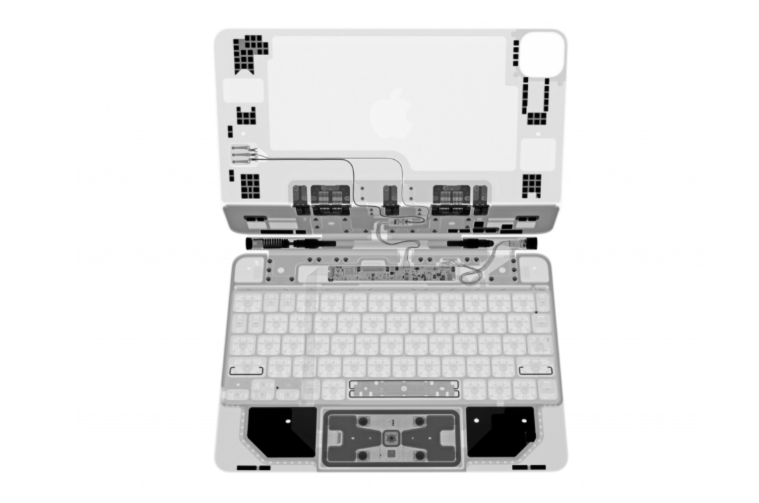
There's a lot going on in this x-ray teardown of the Magic Keyboard for the iPad Pro. (@iFixit) ifixit.com/News/41291/dan…
English