Ayman

217 posts

Ayman banner
Ayman

Ayman

@aymnaus

Australia Katılım Ocak 2026
224 Takip Edilen55 Takipçiler
Ayman retweetledi
AlmaCap
AlmaCap@AlmaCap114204·
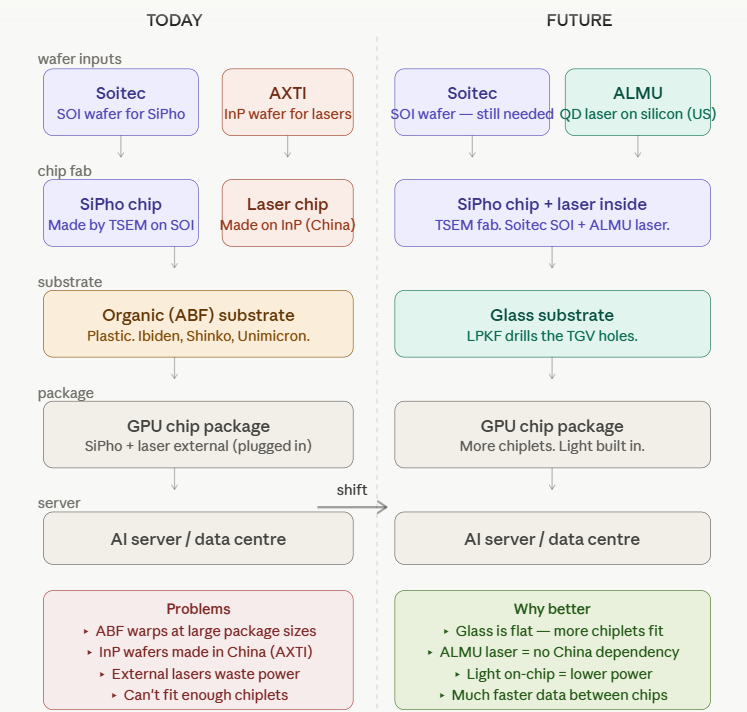
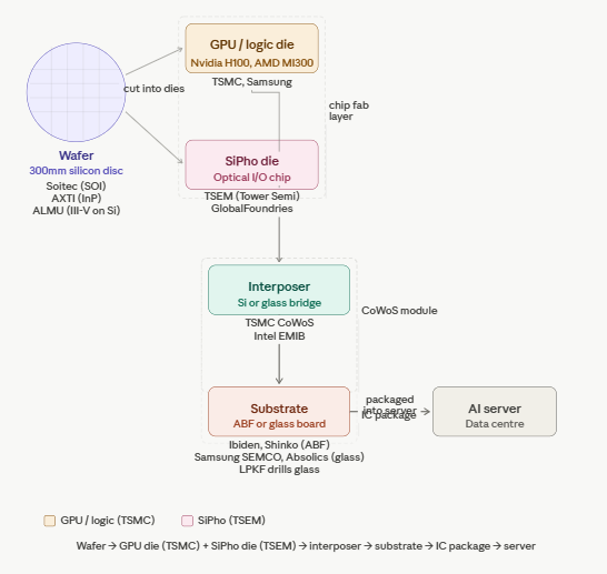
AI chip packaging is confusing, here's another diagram to help Two types of die live inside the same next-generation package: - Logic die (GPU/ASIC): the compute engine, performs the calculations. Typically made by TSMC. - SiPho die: the optical chip (photonics), converts electrical signals into light and back again, so data moves between chips at the speed of light rather than crawling through copper. Made by specialist foundries including TSEM (Tower Semi). $TSEM $SOI $AXTI $ALMU $LPK $TSMC
AlmaCap tweet media
AlmaCap@AlmaCap114204

Photonics is a bit confusing, hopefully this simplified summary helps. I have positions in $TSEM, $SOI, $ALMU, $LPKF

English
3
8
70
10.3K
Ayman retweetledi
tae kim
tae kim@firstadopter·
SK Hynix is back to SK Hynix-ing
tae kim tweet mediatae kim tweet media
English
4
2
74
20.3K
Ayman retweetledi
Ali Behrouz
Ali Behrouz@behrouz_ali·
The growing KV-cache of attention is the key component for the long-context understanding of LLMs, but what holds back long-term memory modules (e.g., Titans)? What if we could have the compression power of Titans but with a growing memory similar to Transformers? Memory Caching: A class of architectures that compress the context into a slow growing memory (not as fast as Transformers, but not as static as RNNs), resulting in recurrent neural networks with non-fixed-sized memory (hidden states). Building on this formulation, we present Sparse Selective Caching, an architecture with growing effective memory (similar to attention) but with almost constant inference cost per token (similar to RNNs).
Ali Behrouz tweet media
English
18
161
979
101.6K
Ayman
Ayman@aymnaus·
Aeluma's quantum dot laser technology (or Quintessent's heterogeneous integration) allows growing III-V laser material directly on silicon in a standard CMOS fab. TSMC fabricates a single chip that contains both the optical circuits and the integrated laser (no separate InP laser chip needed) This unified photonic chip is mounted on a glass substrate (TGVs drilled by LPKF, glass from Corning/AGC/Schott) instead of organic ABF. The glass substrate stays flat, allowing far more chiplets per package. Optical waveguides can be embedded in the glass itself for additional routing. The result is a GPU package with optical I/O built in from the start (not an afterthought plugged in at the edge). Data moves as light from the moment it leaves the GPU die, through the package, through the fibre, to the next switch or GPU. No copper bottleneck anywhere in the path. This enables 60-80mm packages with 8-16 chiplets, petabit-per-second connectivity per rack, 70% reduction in networking power, elimination of Chinese InP laser dependency, and simplified assembly with fewer discrete components.
AlmaCap@AlmaCap114204

Photonics is a bit confusing, hopefully this simplified summary helps. I have positions in $TSEM, $SOI, $ALMU, $LPKF

English
0
0
1
47
Ayman retweetledi
AlmaCap
AlmaCap@AlmaCap114204·
Photonics is a bit confusing, hopefully this simplified summary helps. I have positions in $TSEM, $SOI, $ALMU, $LPKF
AlmaCap tweet media
English
16
118
745
72.5K
Ayman
Ayman@aymnaus·
Aelauma recently implemented a monolithic integration of quantum point lasers on the SiPhPIC platform, including SiN convolution couplers and waveguides, cascading Si ring resonators, and SiN DBRs. The improvements in coupling efficiency and laser performance are largely due to this MOCVD + MBE hybrid growth strategy. The output power behind the SiN waveguide reached 1.5 mW, and coupling losses were reduced from more than 7 dB to less than 6 dB. These results mark a major breakthrough in scalable monolithic quantile point gain integration on foundry 300 mm SiPh wafers, providing a new paradigm for high-performance, low-power optical interconnects.
English
0
0
2
60
TheValueist
TheValueist@TheValueist·
$ALMU Aeluma: Scaling Compound Semiconductors for Commercial Photonics and Investment Thesis. Aeluma, Inc., is a semiconductor company focused on integrating high-performance compound materials with silicon manufacturing. The firm has the technical potential to disrupt markets like mobile sensing, AI infrastructure, and defense by offering superior performance at a significantly lower cost. While government contracts currently provide a vital financial bridge and validate the technology's physics, the company faces substantial execution risks as it attempts to transition into high-volume commercial production. Management quality is viewed as technically superior but commercially unproven, with recent strategic hires intended to address gaps in manufacturing and business development. Ultimately, the company is framed as a high-upside investment option whose value depends on proving it can scale its laboratory innovations into repeatable, profitable industrial outcomes.
TheValueist@TheValueist

x.com/i/article/2043…

English
2
5
19
10.6K
Jukan
Jukan@jukan05·
FormFactor and MPI vie to break SiPh test bottleneck as ficonTEC reportedly exits As AI data centers officially enter the silicon photonics (SiPh) era, the industry faces severe challenges in testing accuracy and throughput on the path toward mass production of co-packaged optics (CPO) technology. This has drawn close attention to upstream test supply chain dynamics. Initially, the probe station market for SiPh chip testing was dominated by a three-way rivalry among US-based FormFactor, Germany's ficonTEC, and Taiwan's MPI(6223.TW). Each partnered with automated test equipment (ATE) suppliers, foundries, and IC design firms to develop solutions. Recent supply chain reports reveal that after China's RoboTechnik completed a cross-border acquisition in 2025, formally making ficonTEC its wholly owned subsidiary, concerns over technology leakage due to the new Chinese ownership led customers to lose confidence. Consequently, ficonTEC lost ground in the SiPh probe station market, ceding share to FormFactor and MPI. However, some industry insiders argue that ficonTEC's Chinese background is not the decisive factor behind its exit. The primary reason remains its lack of experience in developing probe stations, failing to master core technologies and resolve customer production bottlenecks effectively. Moreover, if ficonTEC is indeed sidelined by leading global players, this could also impact Teradyne, which closely collaborates with ficonTEC, potentially disrupting future product strategies in SiPh test equipment. The testing process for SiPh chips reportedly spans four main phases from wafer level to module packaging: photonic integrated circuit (PIC) testing, wafer-level optoelectronic integration testing, optical engine testing, and post-CPO packaging testing. An industry insider describes the second phase as a "major black hole" in the SiPh manufacturing flow. Currently, only engineering prototypes exist without automated solutions suitable for mass production, resulting in insufficient scale benefits and inadequate test capabilities. MPI stated that urgent demand for SiPh testing over the past two years, driven by CPO packaging's optoelectronic integration needs, prompted it to consolidate its LED and advanced semiconductor test (AST) product lines by 2026. This move aims to accelerate development in optoelectronic measurement technologies while maintaining close cooperation with Advantest and Keysight. Experts emphasize that before full-scale mass production of SiPh chips can be realized, multiple standardization challenges remain in electro-optical testing processes. This highlights the importance of shift-left testing, since failures in highly integrated CPO packaging are costly, making stage-by-stage validation critical to protecting profit margins. Notably, sources indicate that if the wafer-level optoelectronic integration test bottleneck persists, customers may skip this step during mass production and proceed directly to optical engine testing, where clear solutions already exist, accepting some yield loss and higher costs to ensure final product shipment success. $TER
English
8
13
117
113.2K
Ayman
Ayman@aymnaus·
$LITE Lumentum Yunhui expert interview key points; Thailand plant operations & shifts: • Construction begins in 2025. • Microsoft and Oracle production shifting from Yunhui to Thailand. • Dongguan facility: nearly 90% of 2025 revenue from Google. 2026 capacity targets: • Dongguan: 1.6 million – 2 million units. • Thailand: 1.5 million – 1.6 million units. • Dongguan total shipments: 2.5 million units. 2027 capacity target: • Thailand: doubling to 3 million – 3.2 million units. Product generation shipment forecasts: • 400G: 500,000–600,000 units (2026), 500,000 units (2027). • 800G: 1.6 million units (2026), 2.5 million units (2027), 2.5 million units (2028). • 1.6T: 500,000 units (2026), 1.6 million units (2027), 3.2 million units (2028). • 1.6T production in Thailand: climbing by +100,000 units per quarter starting Q2 2026. Related production financials: • Gross profit margin target: 35% for 1.6T mass production. • 1.6T unit price: dropping from $1,000–$1,100 currently to $900 by 2028. • Early 1.6T production yields: low but do not impact delivery schedules.
English
0
0
3
153
Ayman
Ayman@aymnaus·
“Recently, media reports have reported that South Korea is using a variety of means, including technological research and development, corporate cooperation and government support. We will actively promote the application of silicon carbide in HBM manufacturing to enhance the performance, reliability, and production efficiency of HBM, thereby meeting the growing demand for high-bandwidth storage chips in fields such as AI and high-performance computing. The Korea SME Technology Information Institute has issued the "Targeted Announcement for Investment and Finance Linkage Technology Development Project for 2026," officially launching the development of the "Silicon carbide monocrystalline high-speed pulse heater for HBM heat and pressure bonding machines." The project will receive up to 5 billion won support, including silicon carbide single crystal heating structure design, Heat transmitter manufacturing and prototype development, electromechanical interface design of HBM bonding equipment, etc., are aimed at developing high-power, high-reliability pulsed heating technology through silicon carbide materials and overcoming key technical challenges in HBM bonded heat. In fact, in addition to being a component of key manufacturing equipment, silicon carbide has the potential to penetrate directly into the packaging structure of HBM and become a core material to break through existing technical bottlenecks thanks to its excellent physical properties. Industry data indicates that due to its exceptional thermal, mechanical, and electrical properties, silicon carbide is poised to become a crucial material for overcoming the limitations in heat dissipation, reliability, and integration in HBM technology, thereby providing vital support for enhancing memory performance in the fields of AI and high-performance computing. HBM uses a 3D stacked architecture, where multi-layer chip stacking results in a dramatic increase in thermal density.The thermal conductivity of silicon carbide is three times that of silicon (370-490 W / m · K), which can quickly transfer heat from the inside of the chip to the outside of the packaging, effectively alleviate local hotspots, reduce chip junction temperature, and improve HBM reliability and performance stability. HBM's 3D stacks place great demands on the mechanical strength of the package structure. The high hardness and strength of silicon carbide can support multi-layer chip stacking, and thanks to its similar thermal expansion coefficient to silicon, it can effectively reduce mechanical stress, reduce reliability risks such as chip cracking and layering, and ensure that HBMs operate stable in complex working environments. The high electrical resistance and dielectric strength of silicon carbide enables more dense cabling, reduces signal transmission losses, and increases data transfer rates and energy efficiency at HBM. At the same time, its excellent electrical insulation performance helps to optimize power management and reduce power consumption. The silicon carbide intermediary layer can serve as an interconnect medium between HBM and computing chips such as GPUs, enabling high-density wiring and high-frequency signal transmission, breaking through the thermal management and mechanical performance bottlenecks of traditional silicon intermediaries, and supporting more complex heterogeneous integration architectures.”
English
0
0
0
55
Ayman
Ayman@aymnaus·
“As of March 26, OpenRouter list of large model weekly calls trend; Openrouter raised the consumption of the top ten global models, domestic Minimax M2.5, DeepSeek V3.2, KimiK2.5 and other models, with ultra-low token, high-performance performance,Having been recognized by the market,API calls account for 50% of the global model.”
English
0
0
1
108
Ayman
Ayman@aymnaus·
@zephyr_z9 Educate me then, I don’t speak Chinese, and depending on WeChat translations and pattern recognition
English
1
0
1
84
Zephyr
Zephyr@zephyr_z9·
Pretty interesting chart from JPM They estimated 125T tokens per day for 2026 (China was already at 140T tokens per day in March) They expect token demand to grow from 45 Quadrillion in 2026 to 4.5 Quintillion by 2030 100x growth in 4 years
Zephyr tweet media
English
10
6
113
11.7K
Ayman
Ayman@aymnaus·
@OMGTheMess You mean the treasurer that had back to back budget surpluses? Alright 👍
English
0
0
3
230
Old Soldier
Old Soldier@OMGTheMess·
Jim Chalmers economy
Old Soldier tweet media
English
19
96
289
11K
Ayman retweetledi
Kaushik
Kaushik@WisemanCap·
$AVGO Google TPU agreements: significantly increases TPU partnership visibility - BofA PT $450 We continue to see $30+ EPS power (incl. SBC) by CY30 as AVGO's custom ASIC programs give multi-year visibility and as AVGO's networking wins more traction. Potential ramps at other customers (such as Meta, OpenAI, Apple, etc.) could also help. AI compute remains our favorite group, with top picks NVDA, AVGO, MRVL, AMD.
English
4
9
66
7.2K
Ayman retweetledi
JT
JT@lokoyacap·
This speaks for itself: "Broadcom Inc. (“Broadcom”) and Google LLC (“Google”) have entered into a Long Term Agreement for Broadcom to develop and supply custom Tensor Processing Units (“TPUs”) for Google’s future generations of TPUs and a Supply Assurance Agreement for Broadcom to supply networking and other components to be used in Google’s next-generation AI racks through up to 2031."
English
1
1
39
4.4K
Ayman retweetledi
MacroValue
MacroValue@pradeeepk·
$AVGO built TPUs better at inference than $NVDA Only $AVGO can match $NVDA in networking $AVGO has near full optics stack inhouse vs $NVDA which needs to source externally As ASICs get more complex in next generations only $AVGO can compete with $NVDA Everyone else $MRVL Mediatek AIchip etc will fallout
English
6
6
37
4.2K