Casas de Pax Spice:
🇺🇸 United States
🇦🇺 Australia
🇬🇷 Greece
🇮🇳 India
🇮🇱 Israel
🇯🇵 Japan
🇶🇦 Qatar
🇰🇷 South Korea
🇸🇬 Singapore
🇸🇪 Sweden
🇦🇪 United Arab Emirates
🇬🇧 United Kingdom
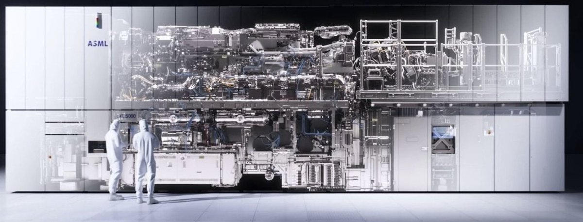
@FutureJurvetson@dch_nl@farzyness Can you / they share yet whether this is proximity printing, mask less direct write, or by some dark arts actually has magnification?
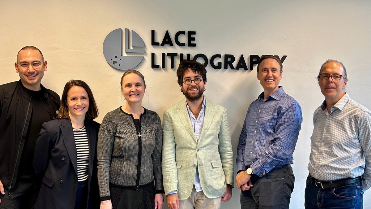
Introducing Ⓛ 𝗟𝗔𝗖𝗘 𝗟𝗜𝗧𝗛𝗢𝗚𝗥𝗔𝗣𝗛𝗬
A novel approach to chip-making that can extend Moore's Law 10x beyond what is possible with light — to atomic resolution.
News today: "Manufacturers use light-based lithography systems made by the Dutch company ASML, which dominates the market. Lace has developed a new approach. Instead of light, Lace's engineers have made a form of lithography that uses a helium atom beam. With that, the Norwegian company will be able to create chip designs that are 10 times as small as what is currently possible"
"The main advantage of the helium atom beam is the industry could create features such as transistors, the building blocks of modern chips, an order of magnitude smaller to an "almost unimaginable" degree, according to John Petersen, Scientific Director of Lithography at Imec, a research and innovation hub for the chip industry.
The beam Lace will use to make chips is about the width of a single hydrogen atom, or 0.1 nanometer. ASML's lithography tools use a beam of light that is about 13.5 nanometers; a human hair is about 100,000 nanometers wide.
Smaller transistors and other features would give chipmakers the ability to ramp up the performance of advanced AI processors well beyond the current capabilities. Lace's technology would enable chip manufacturers to print wafers at what is "ultimately atomic resolution" — reuters.com/world/asia-pac…
Now hiring in Bergen and Barcelona: LaceLithography.com
@NickParkerPrint@FutureJurvetson@dch_nl@farzyness The bottom right image on the first tweet suggests mask, but with gas field ionisation you get a highly collimated beam. So a mask doesn't make sense.
@r0ck3t23 Yeah good luck i remember all the 4680 claims in 2020 which were never achieved. Elon is dependent on fab eqpt suppliers they will want to see cash and not hollow claims. If you do the downpayment they will build.
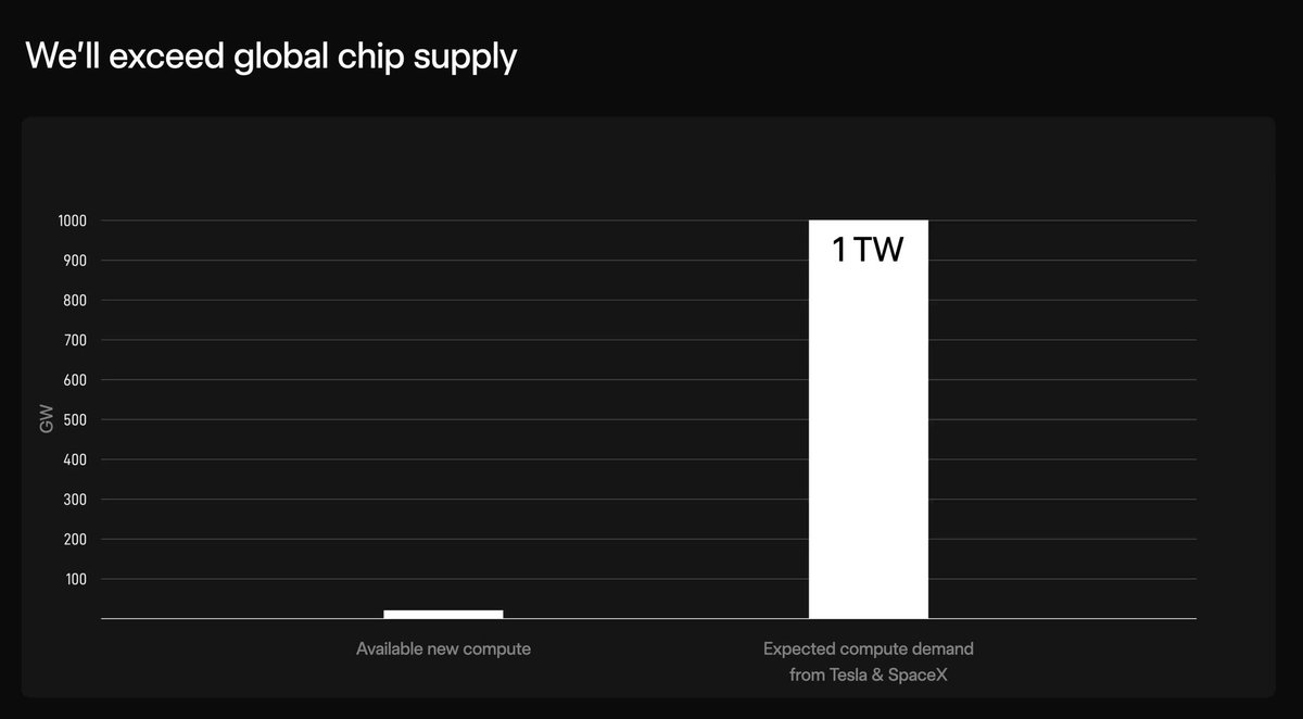
Elon Musk just revealed a number that should end every semiconductor debate on the planet.
Two percent.
Musk: “All the fabs on Earth combined, they’re only about 2% of what we need.”
Every TSMC node. Every Samsung facility. Every Intel foundry. Everything this planet has ever built to make silicon.
Two percent.
The entire global chip supply chain that nations go to war over. That companies wait quarters to access. That built every phone, every server, every GPU you have ever touched.
It covers two percent of what the intelligence explosion actually requires.
That is not a bottleneck. That is a rounding error pretending to be an industry.
Musk: “We will buy all of their chips. I have said these exact words to them.”
He is not competing with TSMC. He is not negotiating with Samsung. He is offering to absorb their entire output.
And it is still not close to enough.
Musk: “There’s a maximum rate at which they’re comfortable expanding.”
There is your problem in one sentence.
The companies controlling the world’s silicon are expanding at the speed of comfort.
The intelligence explosion does not move at the speed of comfort. It moves at the speed of consequence.
And the gap between those two speeds is called Terafab.
Musk: “We either build the Terafab, or we don’t have the chips. And we need the chips. So we’re going to build Terafab.”
No fundraising roadshow. No pitch deck. No permission. We need the chips. So we build the factory.
That is the entire decision tree. And he already chose.
The rest of the industry spends years modeling risk, consulting boards, hedging timelines.
Musk did the math, saw a 98% deficit, and broke ground.
The companies currently celebrating a new fab that increases global output by a fraction of a percent are celebrating a rounding error. They are filling a swimming pool with an eyedropper while Musk is redirecting the ocean.
Two percent is not a starting point. It is an indictment of every industrial plan that came before this moment.
And Terafab is not the answer to a chip shortage.
It is the answer to the question nobody else was willing to ask.
What happens when one company needs more silicon than the entire planet currently produces.
You build the planet’s output yourself.
Terafab's decision to bring the mask shop inside the fab is not a game changer and it certainly doesn't exponentially speed up the development process. The "iterative loop" with the lithography masks that Elon was talking about last night is the design-for-manufacturing (DFM) loop.
In short, this is using the mask to pattern a particular chip layer, for example, metal-1, then inspecting the outcome in various ways to identify repeating issues in the mask design. Then the software used to make the mask can be updated to fix the issue. This process loop repeats over and over again to remove yield-impacting defects from the pareto charts for each module.
DFM is the most common form of fab change control because the many FMEA pieces are automated and not subjective like a physical process change would be—as in new failure modes are not up to the process engineers' imagination. With DFM, the likelihood that a mask change will create some new type of defect is very low, but this comes at the price of doing extensive verification by software means.
The benefit a fab gets from bringing the mask shop in-house is minimal, only affected by the shipment of the mask itself, which is typically 1 day. This is but a small part of the DFM loop that typically takes a month or more. I put some back-of-envelope numbers for each step, and in the best case, this could be shrunk down to something like 10 days, but that would be a very rare occurrence in the chip development cycle. Keep in mind advanced lithography masks can cost $100-200k so there is also a big cost penalty to making a mask that would be DOA.
My flowchart here is a very simplified depiction of this process, but it gives you an idea of how complex the loop can get for DFM.
The biggest fumble in business ever might be Philips spinning off ASML, TSMC and NXP
Philips co-founded ASML in 1984, then co-founded TSMC in 1987, then they founded NXP
They sold each of them for short term profits in the 2000s
ASML is now worth $545B
TSMC is worth $1.76T
NXP is worth $50B
Philips today is worth just $27B
If they'd never sold, Philips would be the largest company in the EU today, worth $650B
Philips CEO Cor Boonstra called it "making money with the success of the past"
🤡