STE

620 posts

STE

STE

@hs_kuo

Semiconductor technology enthusiast

Taipei Katılım Nisan 2013
378 Takip Edilen646 Takipçiler
STE
STE@hs_kuo·
@Meito_1 @meng59739449 4 layers Ribbonsheet is ready now? I am surprised who has it now? The mainstream is 3 sheets solution
English
0
0
0
17
Muxim
Muxim@Meito_1·
@meng59739449 I wonder why A13 name exists at all why not A14P? As they always do This all started when they renamed N2P to A16 so their nodes can look better compared to similarly named Intel nodes, but now it have created this absurd in naming
English
1
0
2
155
meng
meng@meng59739449·
TSMC New Node Roadmap Update 1)A16 confirm delay until H2 2027 2)BPSDN and 4-layer Nanosheet GAA technology behind intel around 2 years 3)A13 is A14 enhanced version node 4)A12 is A14 BSPDN version node
meng tweet media
English
1
6
56
3.3K
STE
STE@hs_kuo·
@Mar364503 If my understanding is correct, his replacement in Samsung foundry -Margaret Han from tsmc has been on board for a few months. It seems not a “captain jump boat”.
English
1
0
1
73
MQ
MQ@Mar364503·
I wonder what attracted him to $INTC given his seniority at Samsung? Normally senior executives would prefer staying with the company where they devoted much of their career to instead of jumping the ship at such seniority. He must have seen something we don’t. I wonder what it is. (I don’t think it is because of money or at least it is not a main driver here.)
MQ@Mar364503

$INTC Hires Samsung Chip Manufacturing Veteran Shawn Han to Aid in Intel Foundry
English
5
7
99
13.2K
STE
STE@hs_kuo·
@christophauto Really? I am wondering how many experienced and high quality customer service, product and integration engineers needed to prevent data visibility becoming daily communication disaster.
English
0
0
0
142
chris
chris@christophauto·
Based on conversations I’ve had along with an analysis of recent hiring trends I’ve seen at Intel $INTC , I’m predicting Lip-bu has a solid plan for IFS to outshine TSMC in several ways, a few of which I’ll list here: 1. Co-design/“Yield-as-a-Service”: Dedicated Customer Yield Engineers and Data Stewards (MDCE roles) would deliver real-time/root-cause analysis and layout recommendations mid production. For example, “your hot spot is from this lithography pattern, here’s the fix for the next tapeout.” While TSMC provides reports or may suggest a third party VCA partner like unichip or AIchip, Intel is planning to act as an embedded co-design team which promises to drastically reduce customers time to market and design costs. In essence, Intel is going to act as an extension of fabless customer’s design teams in a way no other foundry is currently offering. 2. Recent uptrend in hiring of foundry data steward/scientist roles along with an insider discussion I had suggests Intel is substantially improving on its current “Intel Foundry Portal” by providing new AI enabled data metrics that go far beyond what TSMC provides customers. Both TSMC’s and Intel’s foundry portals provide the basic lot tracking, order status, WAT reports, SPC charts, etc, but Intel is planning to start providing advanced data that TSMC does not currently provide like predictive binning forecasts, defect density maps/performance projections that provide summarized/secure views of inline issues with suggested tweaks for the next tape out (for example: “top-left quadrant running 8–12% hotter due to intra-field CD variation, here’s the suggested tweak we recommend”). Offering the higher level granular, predictive transparency that Intel foundry will provide customers promises to give the customer a high level competitive advantage in optimizing their next tape out and reducing time to market. 3. Built in “Trusted Data Environment:” Intel has heard customer concerns regarding providing their IP to a potential competitor and they’re implementing isolated partitions within the company where only select MDCE teams ever see customer data. While customers still get full insights and design assistance, Intel never sees customer’s proprietary architectural secrets. Basically, what I’ve learned is that Intel under LBT is leaning hard into Pat’s “systems foundry” differentiation while tweaking it in his own way by providing much deeper co-design and richer data services, while also addressing customer concerns regarding IP protection by creating more explicit firewalls within the company. Lip-Bu’s strategy in the past has been to talk to potential customers every single day and find out what he can provide to them that they want but aren’t currently receiving from their supplier. This is exactly what he’s doing here. TSMC is an execution machine, but Intel is finding clear ways to differentiate itself.
English
10
33
236
31.3K
GhoneCapital
GhoneCapital@GhostCapitalBoo·
@jukan05 The issue is that in 3 years when they will adopt Hi Na, they won't have the capacity because they will not have already migrated some of their customers. It will all come at once. They will lose many customers to $INTC which is an early adopter.
English
1
0
5
1.4K
Jukan
Jukan@jukan05·
TSMC said in its meeting with Bernstein that it will not adopt high-NA EUV for A16 or A14. $ASML
English
21
17
286
69.2K
STE retweetledi
Fractilia
Fractilia@fractilia·
In high-volume DRAM manufacturing, catching a yield-impacting event early can make all the difference. In our latest from #SPIELitho 2026 — can stochastics measurements from CD-SEM images outperform traditional CD and defect metrics for yield prediction? fractilia.com/public-academy/
Fractilia tweet media
English
0
1
2
93
🌿 lithos
🌿 lithos@lithos_graphein·
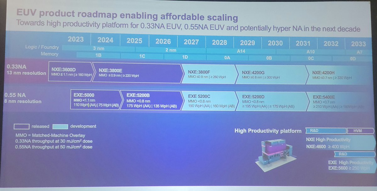
If you're paying a 20% premium to expedite your 3800E orders, there's always the option of paying a 150% premium to get a 5200B.
🌿 lithos tweet media
English
4
1
40
3.4K
STE retweetledi
Fractilia
Fractilia@fractilia·
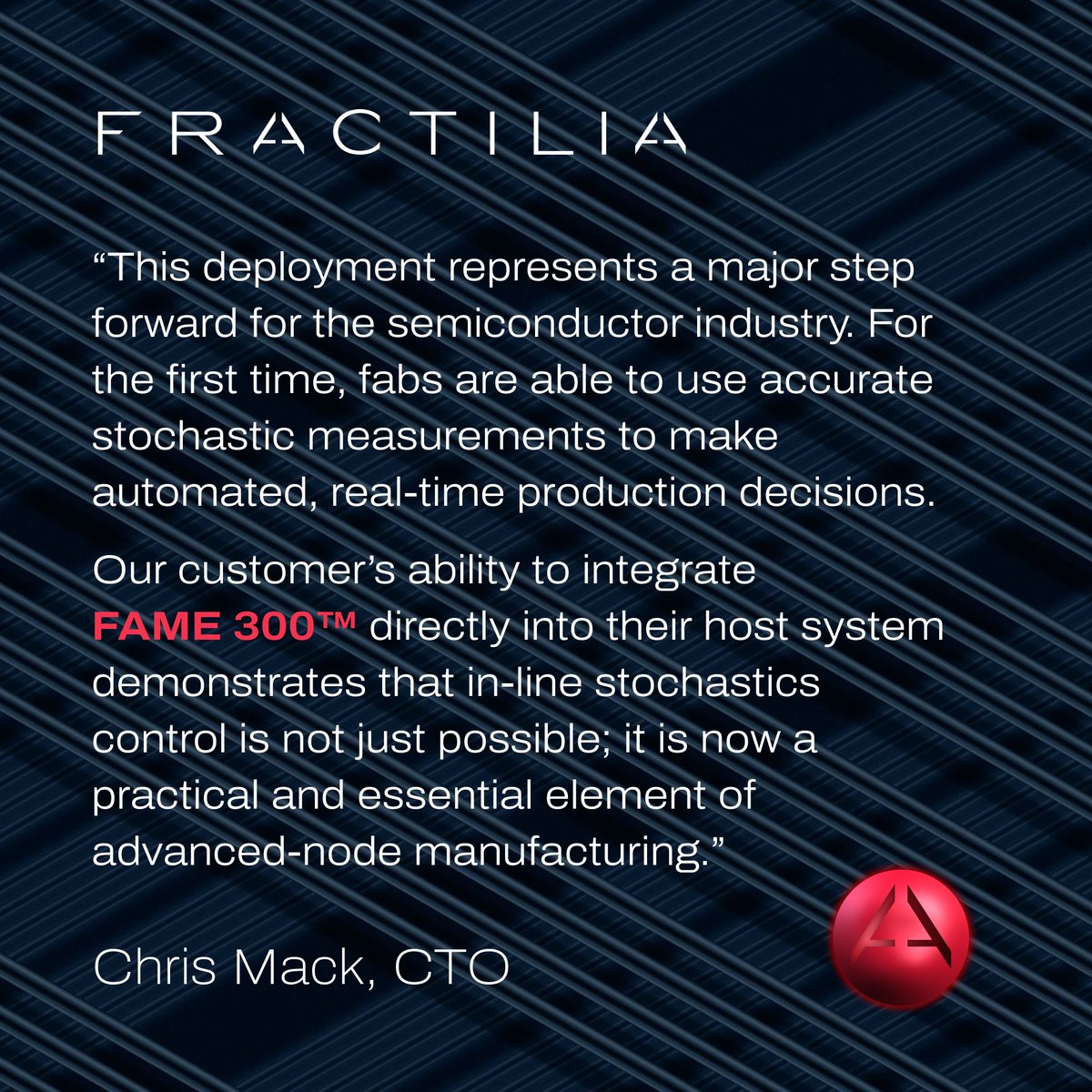
Fractilia's FAME 300™ is now deployed in production at a top-5 semiconductor manufacturer — fully automated, fully integrated, and running across 200+ metrology steps. The stochastics era of manufacturing is here. Read more: fractilia.com/news
Fractilia tweet media
English
0
1
3
107
STE
STE@hs_kuo·
@mingchikuo The most common comment I heard from executives sometimes will be like: “Dude, it is not number, it is a big big money. You should have profit and return in your mind first!”
English
0
0
0
243
郭明錤|Ming-Chi Kuo
郭明錤|Ming-Chi Kuo@mingchikuo·
My latest supply-chain surveys indicate that Carl Zeiss SMT will significantly expand its EUV and higher-ASP immersion DUV optical system capacity by 20-25% YoY and 40-50% YoY, respectively, in 2027 to meet robust demand from ASML. Coupled with stronger-than-expected shipment outlooks for 2026, ASML's revenue is projected to reach €38–40bn in 2026 and €45–47bn in 2027, outperforming market consensus of ~€34–36bn and ~€41–43bn. Key drivers behind the upside vs. consensus are as follows: 1. 2026 Growth Drivers: ➢ EUV and DUV shipments are estimated at 67 and 355 units, surpassing consensus of 53–55 and 310–320 units. ➢ Driven by strong 2nm demand, TSMC has upwardly revised its 2026 EUV orders twice: from an initial 22 units to 25 units last October, and currently to 28 units. ➢ To capture robust demand from Chinese memory makers, ASML plans to launch a new immersion DUV model NXT:1965i in 4Q26. As a down-spec version of the 1980i series, it complies with U.S. export controls while addressing Chinese clients' needs, serving as a key growth driver for 4Q26 and 2027. 2. 2027 Growth Drivers: ➢ 2027 capacity for both EUV and immersion DUV is currently fully booked thanks to the strong demand; further shipment upside will hinge on ASML’s supply-side improvements. ➢ Based on Zeiss SMT’s expansion, ASML’s 2027 shipments are projected to reach 80–85 EUV systems and 380–400 DUV systems. ➢ Boosted by the new 1965i launch, China’s procurement of high-ASP immersion DUV is expected to grow ~40% YoY in 2027. 3. Additional Upside Potential to Monitor: ➢ Potential ASP hikes for EUV and DUV systems amid prolonged supply tightness. ➢ Ongoing upward revisions for the new 1965i model from Chinese memory suppliers. ➢ Potential Intel Upside: The above estimates exclude incremental EUV demand from Intel. Although Intel has not officially placed orders (explaining its previously lower-than-expected Capex guidance), it has entered discussions with ASML for additional bookings. Intel's incremental EUV demand is projected at 20–30 systems over 2026–2027, of which 3–5 are High-NA EUV.
English
11
60
417
242.4K
STE
STE@hs_kuo·
@jukan05 “introduce the key component 'Extreme Ultraviolet (EUV) Pellicle' to enhance productivity ” Interesting and the first time I hear the comment about EUV pellicle will enhance productivity. EUV light will pass Pellicle twice which absorbs light and typically costs productivity.
English
0
0
0
72
Jukan
Jukan@jukan05·
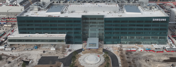
Samsung Introduces 'EUV Pellicle' First in US Taylor Fab... Mass Production Imminent Samsung Electronics will first introduce the key component 'Extreme Ultraviolet (EUV) Pellicle' to enhance productivity in advanced semiconductor processes at its Taylor fab under construction in the US. Although its adoption had been unclear until now, the company has essentially confirmed it by placing orders for key equipment. According to industry sources on the 22nd, Samsung Electronics has ordered EUV pellicle facilities for its Taylor fab in Texas, USA. FST has secured a contract worth 25 billion won to supply EUV pellicle attachment/detachment equipment and inspection equipment. The EUV pellicle is an ultra-thin protective component mounted on the photomask during the exposure process. Semiconductors are created by shining light onto a photomask with pre-drawn circuits to transfer them onto the wafer. Applying the EUV pellicle prevents fine particles or contaminants from adhering to the photomask surface, thereby mitigating yield reductions. To use the EUV pellicle in exposure equipment, dedicated tools for attachment/detachment and inspection equipment to check its condition are required, and these will be introduced to the Taylor fab for the first time. The FST equipment supports not only next-generation carbon nanotube (CNT) EUV pellicles but also existing metal silicide (MeSi) EUV pellicles. Previously, competitor TSMC has been gradually introducing Mitsui Chemicals' metal silicide EUV pellicle since 2019 and applying it to advanced processes. Samsung Electronics has been pushing for the localization of EUV pellicles by investing in S&STech and FST in 2020 and 2021, respectively. With this latest equipment investment, it is analyzed that sufficient performance has been achieved, signaling that adoption is imminent. This implies that the pellicle's key performance metrics—durability and transmittance—have reached satisfactory levels. An industry official stated, "The quality evaluation of the EUV pellicle is currently ongoing, but the introduction of equipment premised on mass production application at the Taylor fab is a positive development," adding, "It is expected to expand to memory processes in the future, starting with system semiconductor processes." The Taylor fab is a semiconductor manufacturing facility that Samsung Electronics is building with the goal of commencing 2-nanometer (nm) mass production in the second half of this year. Tesla's artificial intelligence (AI) chip 'AI5' is also slated for mass production there within the year. Samsung Electronics currently possesses over 70 EUV machines, ranking second after TSMC. As such, the adoption of domestically produced EUV pellicles is expected to have a substantial ripple effect on the equipment and components industry. The price of an EUV pellicle is estimated to be over 60 million won.
Jukan tweet media
English
9
15
139
40.4K
STE
STE@hs_kuo·
@austinlyons Sometimes it is hard to compare the readiness of tech file names with different time line definition now. But customers’s feet prove the story.
English
0
0
1
115
Austin Lyons
Austin Lyons@austinsemis·
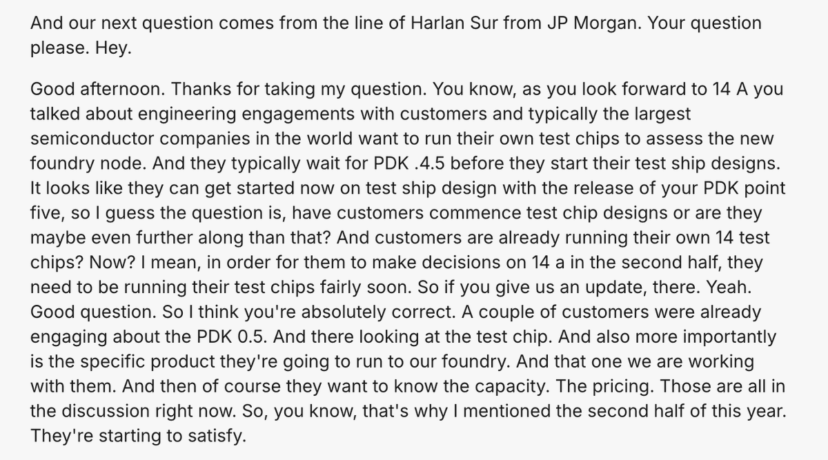
A few prospective 14A customers have test chips in hand already.
Austin Lyons tweet media
English
5
8
81
14.6K
STE
STE@hs_kuo·
@meng59739449 I checked the date. April 1st is still months away and it seems someone pulls in it.
English
0
0
2
421
meng
meng@meng59739449·
Rumor 18A new Yield : 70% , cost/per wafer : 16500 USD N2 new Yield : 60 - 70% , cost/per wafer : 22000 USD node learning curve (lab to product) : 18A - 18 month , N2 - 24 month Chip Area 18A scaling than 22% N3
English
19
34
388
30.6K
STE
STE@hs_kuo·
@jukan05 Currently, A’s 2nm even using the same GAA architecture is different from B’s and C’s. The yield comparison is more or less like comparing tangerine to orange. If the yield gap of “the same design” is less than 20%, it will be economic not technical decision.
English
0
0
0
56
Jukan
Jukan@jukan05·
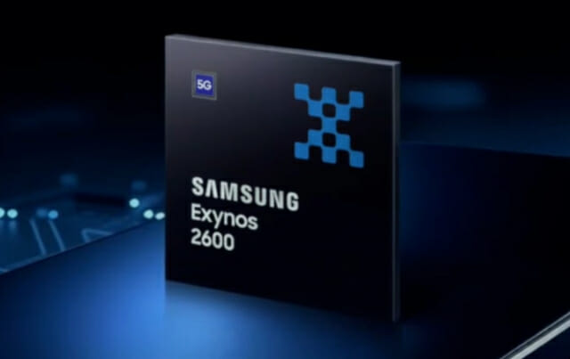
Samsung Electronics Achieves 50% Yield in 2nm Process, Intensifying Pursuit of TSMC TSMC is widening its "super-gap" lead in the cutting-edge foundry market. Following a significant increase in the revenue share of its 3nm process in Q4 last year, the company plans to fully scale 2nm mass production this year. Meanwhile, Samsung Electronics is closing the gap, successfully raising the yield of its first-generation 2nm process to the 50% range. Samsung is also actively preparing for future growth by directing partners to aggressively promote its second-generation 2nm process. On the 15th, during its Q4 earnings conference call, TSMC disclosed the current status of its advanced process development and commercialization. TSMC: 2nm Ramp-up This Year; Next-Gen Processes on Track TSMC CEO C.C. Wei stated, "The N2 (2nm) process successfully entered mass production in the second half of last year, and we expect a rapid ramp-up this year based on our continuous performance improvement strategy." The N2P process, an enhanced version of N2, is also scheduled for mass production in the second half of this year, offering superior performance and power efficiency. Furthermore, the 16A (1.6nm) process, which incorporates proprietary Backside Power Delivery Network (BSPDN) technology, will also begin mass production in the same period. BSPDN improves chip performance and design flexibility by placing power delivery lines on the back of the wafer. Industry analysts believe TSMC’s 2nm process secured stable yields from the early stages of production, with some local reports in Taiwan suggesting yields are already exceeding 80%. Consequently, TSMC is expected to maintain its dominance in the advanced foundry market this year. As of Q4 last year, 3nm process revenue accounted for 28% of TSMC’s total sales, marking a record high. Samsung Electronics: Catching Up with Improved 2nm Yields Samsung Electronics also began mass production of the 'Exynos 2600'—its latest mobile Application Processor (AP) based on the first-generation 2nm (SF2) process—in Q4 last year. The Exynos 2600 is expected to be featured in the 'Galaxy S26' flagship series, scheduled for release in Q1 this year, alongside Qualcomm's latest chipsets. Industry sources estimate Samsung's wafer-level yield for this process to be in the 50% range, a significant improvement from the 30% range seen in mid-2025. Unlike its predecessor (Exynos 2500), no fatal defects occurred during the initial mass production phase. A semiconductor industry insider noted, "While specific figures may vary based on binning criteria, the Exynos 2600 yield has reached a relatively stable level in the 50% range. The MX (Mobile eXperience) division is encouraging the use of this chipset, which is expected to account for approximately 25% of total Galaxy shipments." Success of SF2P Process as the Key: "Promotion Guidelines Issued to Partners" However, the consensus within the industry is that the success of the second-generation 2nm (SF2P) process is critical for a full-scale rebound of Samsung’s foundry business. Compared to SF2, the SF2P process offers a 12% increase in performance, a 25% improvement in power efficiency, and an 8% reduction in area. Another industry source shared, "Samsung has poured immense effort into developing SF2P based on the SF2 foundation and completed the basic Process Design Kit (PDK) in mid-last year. Recently, they reportedly issued guidelines to Design Solution Partners (DSPs) to actively promote SF2P, rather than SF2, to potential customers." Potential customers are closely monitoring the success of SF2P, as it will be used for both Samsung’s next-gen Exynos 2700 and Tesla’s AI semiconductors. Samsung previously secured a 22 trillion KRW foundry contract with Tesla to produce the 'AI6,' a high-performance system semiconductor used in Tesla's next-gen FSD (Full Self-Driving), robotics, and data centers. The AI6 chip is known to adopt Samsung’s SF2P process. Samsung plans to produce initial samples at its domestic foundry and packaging facilities before transitioning to full-scale mass production at its new foundry fab currently under construction in Taylor, Texas. "The SF2P process is the first 2nm node for which Samsung has officially secured large-scale mass production from an external customer," an industry expert commented. "Successful production of this chip will be a crucial reference for other customers to entrust Samsung with their own mass production needs."
Jukan tweet media
English
11
25
267
61.9K
STE
STE@hs_kuo·
@lithos_graphein The typical comparison subjects are penny, hair, red blood cell, corona virus, DNA double helix, silicon atoms.
English
0
0
1
68
🌿 lithos
🌿 lithos@lithos_graphein·
Love the old-school printing link here. The semi industry does have its roots in the newspaper printing biz from the late 1800s. It's basically a mass production printing process on steroids. Interesting they use the Red Blood Cell size comparison. I've used it often to describe things in modern litho terms, but I forgot the original source.
ASML@ASMLcompany

Our extreme ultraviolet (EUV) lithography systems print features just 13 nm wide – orders of magnitude smaller than the letters in even the densest books – because that’s the level of detail and complexity needed to make today’s advanced chips a reality.

English
5
3
82
9.8K
STE
STE@hs_kuo·
@meng59739449 Money is the King. In Foundry, yield is the Queen.
English
0
0
1
203
STE
STE@hs_kuo·
@mzuhair123 If there is no definitely “NO”, then everything is possible. Historically, in the preparation stage of the future foundry switch, it takes more than 18 months to start volume relocation after first product validation. I am waiting for the T0 time arrive first.
English
0
0
1
81
Muhammad Zuhair
Muhammad Zuhair@mzuhair123·
Intel Foundry customers are currently evaluating the 18A-P node, based on my understanding. This is a rough estimate of potential customers, derived from the progression of PDK sampling and its positive outcome. - Apple - MediaTek - Microsoft - Google (an unconventional bet, but I have my research on it) These customers are looking for Intel capacity for products that aren't "too mainstream" to be fabbed at TSMC. One of the reasons Intel Foundry sees external momentum is due to the supply constraints faced by TSMC.
Jukan@jukan05

Is this for real? Intel Foundry has already secured four customers for 18A? $INTC

English
12
9
137
21.2K
STE
STE@hs_kuo·
@IntelProMUltra Historically, it could take times to adopt new nodes into high volume even after validation of first test vehicle. Example, it said Apple validated tsmc N28 when Samsung was Apple’s sole supplier then. But Apple’s real volume manufacturing started two years in N20.
English
0
0
1
38
Intel Pro Max Ultra
Intel Pro Max Ultra@IntelProMUltra·
It could be a bad sign, but there are many things to clarify. Since 18A was never intended to serve external customers initially, its PDK maturity was poor (Intel products don't use industry-standard EDA tools; they have their own design automation team), causing suffering for both Intel and external customers. And technically, you're correct, but I don't think Intel needs to "replace" a major foundry. For Intel, winning big deals is difficult until it's technologically competitive with TSMC. For fabless, it's still risky to entrust critical products to Intel due to its IDM model and poor delivery track record. I think these are business problems.
English
1
0
2
102
Intel Pro Max Ultra
Intel Pro Max Ultra@IntelProMUltra·
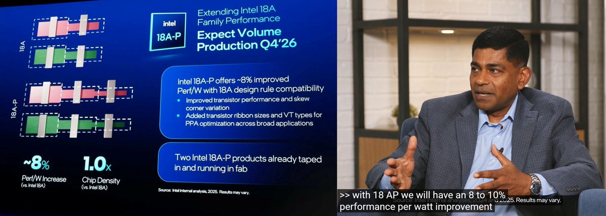
Before you say “18A is internal and 14A is the real game,” don’t forget another killer node, 18A-P, which Intel targets to compete with N2. PPA: 18A is N3P-class in performance but likely has better power efficiency as PTL consuming 30% less power than ARL/LNL. 18A-P brings an additional 8-10% performance uplift over 18A, while N2 boosts 5-10% over N3P. Thus, 18A-P should be competitive with N2. Maturity: 18A to reach industry-standard yields in 2027, where 18A-P will ride that learning curve instead of resetting it. PDK maturity is also better and on track. Timing: 18A-P HVM starts in H2 2026 to support Nova Lake launch, aligning with N2’s first big wave (A and M-series) in H2 2026. I think 18A-P still plays a critical role in landing customers for 14A.
Intel Pro Max Ultra tweet media
English
6
8
105
8K
STE
STE@hs_kuo·
@IntelProMUltra If nVidia stop evaluating 18A, then it was a bad sign and could be more conservative for 14A adoption. From my past experience, it will take more than 2 years to replace major foundry.
English
1
0
1
69
STE
STE@hs_kuo·
@IntelProMUltra Be honest, I am confused by the terms created in the past, like production ready, risk start, HVM….. Typically, it will take more than 9 months from real product tapeout to risk start and even longer for real high volume production.
English
2
0
1
203
STE
STE@hs_kuo·
@IntelProMUltra Great to hear this. Upon this prediction, it seems Intel will get many low NA and Hi NA EUV scanners soon and ASML will have big revenue growth?
English
0
0
2
198
Intel Pro Max Ultra
Intel Pro Max Ultra@IntelProMUltra·
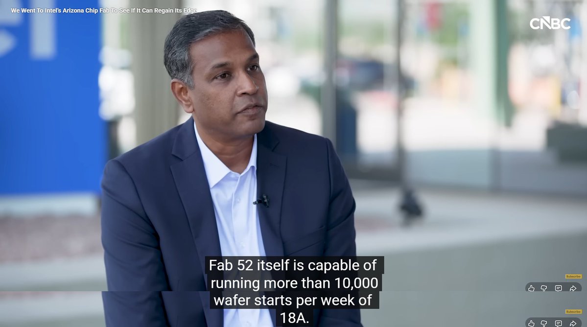
I said this back in February: Arizona Fab 52/62 is a ~40K WSPM-class ramp, and Fab 52 should reach HVM in 2H’25. Now CNBC basically puts it on camera for everyone. In their interview, Naga Chandrasekaran states clearly: “Fab 52 itself is capable of running more than 10,000 wafer starts per week of 18A.” That statement alone implies Fab 52 can produce >40K WSPM (per month). CNBC also mentions that Arizona will have “at least 15 EUV systems.” The nuance is “at least.” because the site is designed to scale: Fab 52 has 2 EUV bays with ~6-tool capacity each (so up to 12 EUV tools), and Fab 62 can mirror that layout (another ~12), implying ~24 EUV tools across Fab 52/62 at full build-out if Intel chooses to fully equip them. Based on what the CNBC footage shows on the fab floor, you can see an EUV bay that currently looks like it has 4 EUV tools installed. The visible mix appears to be 3× NXE:3600D + 1× NXE:3800E. The latter system, provides ~40% higher productivity vs. 3600D due to a higher-power source and a faster wafer stage architecture that shares design with High-NA EXE platforms. More importantly, the bay spacing and the way the infrastructure is arranged looks like a 6-slot EUV bay. In other words, 2 positions appear open, likely reserved for additional NXE:3800E installs. From my understanding, Fab 52 likely has more than just the 4 EUV tools visible in that one bay, which would imply the second EUV bay also houses multiple tools. The footage is not the full fab. But even with only the on-camera evidence, the direction is clear: Fab 52 is set up for a serious 18A ramp. With 18A ramping and Intel 7 still supply-constrained, Intel is walking back its CapEx-down narrative. They initially pointed to ~$15B CapEx in 2026, but now the tone is shifting toward ~$18B plus or minus $1B.
Intel Pro Max Ultra tweet media
Intel Pro Max Ultra@IntelProMUltra

@Mojo_flyin @meng59739449 F52/62 is gonna be 40K And F52 is actually set HVM in 2H25, which I believe the end of 2025, though

English
7
6
58
8.9K