josiah_lee

158 posts

josiah_lee

josiah_lee

@josiah_leee

Katılım Mayıs 2025
83 Takip Edilen729 Takipçiler
josiah_lee
josiah_lee@josiah_leee·
@teortaxesTex Why is that the case? What are the particular properties of Rust that make it so LLM-friendly? I thought Rust was just a memory-safe C that has really good compiler errors? The old saying was "if it compiles, it's basically right." Is that it, or am I missing something?
English
0
0
0
121
Teortaxes▶️ (DeepSeek 推特🐋铁粉 2023 – ∞)
Using agents to code in Rust is qualitatively different from most other languages because the efficiency INCREASES as the session goes on. They learn a lot in-context, they start making more considered targeted edits. It feels… premium.
Eric S. Raymond@esrtweet

In the age of AIs, Rust is the new assembler, and that's how I'm using it. I don't particularly like Rust. I have never hand-coded a single line of the language, and probably never will. Rust's developer and advocate community contains a lot of crazies I don't want to be anywhere near. Nevertheless, I've shipped two Rust projects so far, I expect to have a third out soon, and I'm planning on a fourth. Why? Since I'm doing all my coding with LLM assistance now, none of the things I dislike about Rust matter much anymore. I don't need to know how to write the language, only to read it enough to understand control flow and spot obvious bogons. And I don't need to deal with the crazies, because my robot friends are smarter than they are. Rust has four properties that make it a good target nowadays: 1. LLMs are good at generating high quality Rust code. 2. Memory safety, memory safety, memory safety. 3. Rust is anal about things like lifetimes that other languages aren't. This means that LLM-translating out of it into a future language that I might like better should be easy, because it's a more exact specification of intended behavior. 4. Repeating: LLMs are good at generating high-quality Rust code. Am I going to use it for everything? Oh hell no. I have a bunch of very nice Golang code that doesn't need to be moved to Rust because Golang is a better fit for its problem domain. And I have a bunch of small Python scripts that don't need to move either. But over time, I expect almost all of my C code will in fact move to Rust. Because memory safety, memory safety, memory safety. Someday, maybe, there will be a language with Rust's virtues that I don't dislike. At which point I will cheerfully translate all my Rust stuff out of Rust. Interlanguage translation is easy and cheap now. I don't necessarily have to like the shape of a tool to recognize when it's good for a job.

English
12
5
115
9.6K
josiah_lee
josiah_lee@josiah_leee·
@teortaxesTex SF VC-funded hype videos - assume fake until proven true. Chinese robotics hype videos - assume true until proven fake.
English
0
0
2
113
Teortaxes▶️ (DeepSeek 推特🐋铁粉 2023 – ∞)
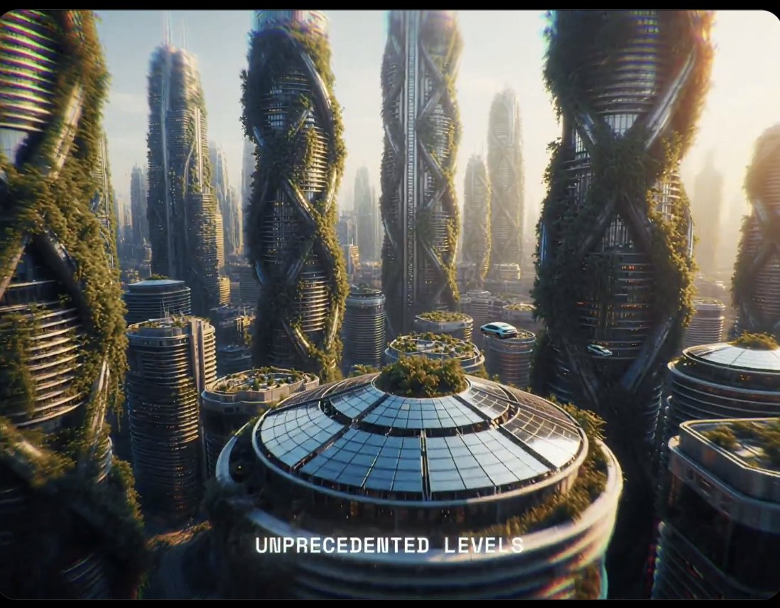
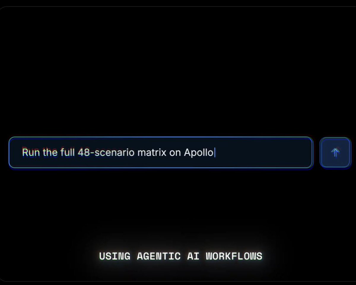
I think it's unserious and in bad taste to mix up real footage, obvious AI slop and unlabeled segments of dubious provenance in a video about your hardware. Far as I can tell, the 1st pic is AI slop. Is the rest of the company the same?
Teortaxes▶️ (DeepSeek 推特🐋铁粉 2023 – ∞) tweet mediaTeortaxes▶️ (DeepSeek 推特🐋铁粉 2023 – ∞) tweet mediaTeortaxes▶️ (DeepSeek 推特🐋铁粉 2023 – ∞) tweet media
Y Combinator@ycombinator

.@ApolloAtomics builds the most compact nuclear reactors with the highest uptime and a deployment time of less than 24 months. Apollo took the pressurized water reactor technology that already powers 80% of the world’s nuclear plants and flipped one part, the steam generator, to make the plant an order of magnitude smaller without compromising power. Congrats on the launch, @AssilHalimi & Drew! ycombinator.com/launches/QXj-a…

English
3
1
56
4.8K
josiah_lee
josiah_lee@josiah_leee·
@teortaxesTex Roman Helmet Guy recognizes the gambit, and is explicitly attempting to deny the support of America and his heritage-Americans (what a linguistic innovation) to Balaji's Network State. He wants a clean break from Balaji and his coethnics. The rest of the argument is just fluff.
English
0
0
4
126
josiah_lee
josiah_lee@josiah_leee·
@teortaxesTex Balaji is smarter and more subtle, but his network state is a gambit to ensure that his coethnics are integrated into whatever future forms. The core contest is between US and China, and China won't let him in. US nationalism is rising, hence the network state in Singapore.
English
3
0
9
306
josiah_lee
josiah_lee@josiah_leee·
@Geiketsu Writes a Chinese post. Japanese user name. Japanese image of 3D flash memory. Glazing Toshiba (which is so cooked that they're delisted from TSE, btw). All signs point to Japanese cope. Hopeless. CNY/JPY to 40 by 2027.
English
0
0
1
54
Geiketsu
Geiketsu@Geiketsu·
什么狗屁LogicFolding啊。不就是当年“SSD固态硬盘”用的3D NAND思路(东芝发明出来那个),现在应用在CPU上吗?而且配图的理解明显有问题,我重新换了张更靠谱的图。 补充:以前SD卡只能单层堆,所以容量很小。后来把NAND多层堆叠,再加并行读写,就成现在应用在“SSD固态硬盘”上3D NAND技术了。
Geiketsu tweet media
墙街研究猿_The Ape of the Great Wall@ApeOfGreatWall

让AI给我解释了一下: 传统芯片升级(摩尔定律)的“老路”是这样的: 想让芯片更快、更省电、塞更多晶体管 → 必须把晶体管画得越来越小(从10nm → 7nm → 5nm → 3nm → 2nm……)。 “画”这么小的线条,只能靠超级贵、超级难的光刻机(尤其是EUV极紫外光刻机)。 
每下一代节点,光刻机都要升级,成本爆炸(一台EUV光刻机上亿美元),设计预算也上10亿刀。 
华为以前被卡脖子,就是卡在这里——拿不到最先进的光刻机,就没法继续“横向缩”。 LogicFolding完全换了一条赛道: 它不缩小晶体管,而是把同一代工艺(固定节点)的电路,像折千层饼一样竖着叠起来! 还是用原来的晶体管大小(不需要新光刻机去画更小的图案)。 把关键的逻辑电路、内存、模拟电路拆开,一部分放在上层硅片,一部分放在下层硅片。 用超级密的“垂直电梯”(混合键合,1.5微米间距)把上下层直接焊在一起。 结果:信号走直达电梯,不用在平面上绕远路 → 线短了30%,RC寄生小了,频率更快、功耗更低、密度更高。

中文
109
15
202
78.4K
josiah_lee
josiah_lee@josiah_leee·
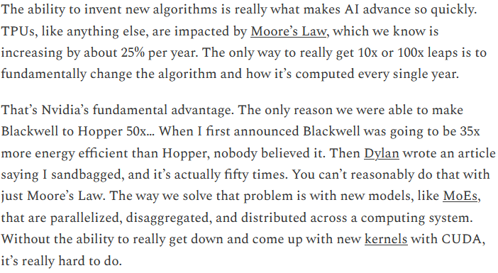
@teortaxesTex Jensen tried to warn them - of the 50x increase from Hopper to Blackwell, <2x was process scaling. The rest was optimizations at other levels. Those other optimizations are just as accessible to Huawei. No EUV required.
josiah_lee tweet media
English
0
3
48
10.2K
josiah_lee
josiah_lee@josiah_leee·
@jukan05 Can't tell if this is being sarcastic or not ... but yes, 1+1 is a 100% increase, 2+1 is a 50% increase, 3+1 is a 33% increase. Yes, very expert opinion, brought to you by kindergarten level math.
English
1
0
3
393
Jukan
Jukan@jukan05·
"However, one thing to keep in mind is that the marginal benefit of this scaling method gradually diminishes. The theoretical gain from folding a single layer into two layers is 100%. But moving from two layers to three layers only adds 50%. If Huawei moves from three to four stacked layers by 2035, the incremental gain would be only 33%. Moreover, as the number of stacked layers increases, the three challenges mentioned earlier — cooling, design complexity, and cost — all become more severe. (…) Leakage also remains unresolved. Cooling becomes increasingly difficult, and the 3D EDA toolchain represents an entirely new challenge. Therefore, Tau scaling is not an exponential growth path that can continue for the next ten years." I’m really grateful to be able to read this kind of expert opinion for free!
fin@fi56622380

华为τ scaling定律营销策略,无非是more than moore的广义摩尔定律的另一种说法而已 作为芯片架构师,我更感兴趣的,还是芯片密度提升,ppt上41%能耗提升和12.7%性能提升,到底是怎么实现的 看完了论文,感觉华为这次创新,本质上是用设计复杂度高 + 高制造成本 + 超前散热,一定程度弥补了工艺差距 ----------------- 1. 华为芯片堆叠带来的等效密度提升,是虚假宣传还是真的,是不是工艺突破?有没有实打实的好处? 等效密度提升的来源,是两片芯片用hybrid bonding技术绑在一起,投影面积理论上能减小一半,但第一代不是全芯片双层折叠,而是选择性折叠关键logic,所以只有大概53%的芯片面积实现了折叠(密度155->238),等到后面几代折叠面积会逐渐增大,到2030年接近全折叠(密度155->292) 这2026第一代等效密度从 2025 年 155 MTr/mm² 跳到 2026 年 238 MTr/mm²,时钟频率也提升了12.7%,功耗比提升41%,表面上看似乎和工艺突破没有什么区别,但有一点重要区别就是leakage power华为从头到尾没有提,只要工艺节点不变,gate leakage、junction leakage 不会因为 3D stacking 自动改善 2030年到2031年的等效密度突变,大概率是来自于2层堆叠到3层堆叠,正如2025到2026年的等效密度突变,时钟频率突变,来自单层到2层折叠 所以从leakage没提这个事来看,这个2031年等效1.4nm,和工艺节点上的突破没有联系。 本质上是用设计复杂度高 + 高成本 + 超前散热 + 超前部署advanced packaging,一定程度弥补了工艺差距 ----------- 那么这样看起来虚假的等效密度提升,有用处吗?好处在哪里? 有的,设计上topology折叠,原来要跑几毫米的水平走线,折叠后变成了几十微米。降低了super buffer/bus的长度,降低了clock tree的深度(clock depth -42%、clock wire -28%),clock skew也带来了改良(-25%),这对动态功耗的改善是实实在在的。部分critical path的缩短,也让时钟频率的上升更容易 所以ppt roadmap上performance的提升,从2025年到2026年上升了12.7%,大部分都是来自于时钟频率的上升(12.7%) 所以好处基本上是topology拆分电路逻辑设计上带来的提升 既然没有实质上的工艺提升,华为芯片堆叠带来等效密度提升的trade off代价在哪里? 三个代价:散热超前发展,设计复杂度高,制造成本变高 最大的代价就是热密度的同步上升,理论上logic on logic都是CPU execution发热最严重的区域,这部分折叠起来相当于功耗密度直接翻倍,但算上41% power efficiency改善,功耗密度仍只比非堆叠方案高40%左右。所以第一代只能对最关键的部分做折叠,大概只占全芯片面积的53%。 所以散热技术也被逼的超前发展,直接上毫米级的MEMS风扇,做micro-cooling fan。 另外的代价就是设计复杂度的变高,critical path的折叠,哪个部分的logic能折叠,折叠之后又会带来从前端到后端的巨大变化要推翻重来 现有的所有EDA工具也不可能支持3D topology,论文自己也承认,full-scale LogicFolding需要全新的3D-native EDA toolchain,把多层stacked dies当作单一连续设计实体处理。哪些logic能折叠、折叠后的inter-die timing closure怎么做,Physical Design(PD)也是难点 制造成本也会更高,被迫超前部署advanced packaging封装,1.5~2um的hybrid bonding + logic on logic都是很有挑战需要显著更高的成本 以前一层wafer做一次光刻;现在两层wafer分别做光刻再bonding,加上hybrid bonding的overlay控制(论文要求<0.5μm)、TSV、KOZ keep-out zone、冗余修复、良率乘法损失,每颗芯片的制造成本和测试成本都要显著上升 -------------------------- 2. Tau scaling这个说法,scaling的到底是什么,这个scaling技术路线是不是一次性的design topology红利?潜力如何?持续进步的空间在哪里? τ Scaling的核心主张是:用时间常数τ替代几何线宽作为全栈优化目标,在器件、电路、芯片、系统四个层级分别压缩特征延迟 公式本身没有任何新物理。"关注瓶颈延迟"是所有架构师都在做的事情。整个行业都知道互联RC是延迟瓶颈,TSMC每一代工艺都在用low-k dielectrics/semi-damascene等手段降RC。把一个众所周知的优化方向包装成"定律"是显然的营销宣传手段,本质是More than Moore的广义摩尔定律的另一种说法 抛开marketing,华为目前所谓RC delay的改善,本质上是芯片堆叠之后,topology距离缩短,让匹配的effective RC都变小,不是RC工艺常数 至于scaling的意思,是能持续发展的一条roadmap。这里的持续改善路径指的是,全芯片堆叠的层数越来越多,从25~30年的2层堆叠,到31年开始的3层堆叠,以后甚至会考虑4层堆叠 第一代折叠技术甚至不是全芯片双层折叠,而是选择性折叠关键logic,所以只有大概53%的芯片面积实现了折叠(密度155->238),等到后面几代折叠面积会逐渐增大,到2030年接近全折叠(密度155->292)。2031年的roadmap之所以会出现一个阶跃,就是因为那是从2层折叠到3层折叠的时间点。 但需要注意的是,这个scaling方法的边际效应是逐渐缩小的,折叠成双层的收益是100%,2->3层的收益就只有50%,如果2035年再从3->4层堆叠,收益就只有33%了 另外随着堆叠层数变高,上面说到的三个挑战,散热,设计复杂度,成本,都是越来越大 --------------------- 3. 华为的芯片堆叠,是不是TSMC/AMD已经有的hybrid bonding技术?华为做到的是cache on logic,cache on cache,还是logic on logic,logic on logic最大的散热问题是怎么解决的? 是已经有的技术没错,但同时也是把现有技术指标做到了领先也是真的,3D堆叠本身不是新技术,TSMC的hybrid bonding量产还是6um,华为论文给出Kirin 2026的hybrid bonding pitch是1.5μm 我在刚刚看到华为的堆叠消息之后,第一反应也是怀疑和AMD的3D V cache类似,它主要把 SRAM cache 叠在 已经有的L3 cache 区域上,通常会避免直接堆在最热的 CPU execution logic 上,就是避免散热问题,毕竟SRAM 的功耗密度和热点特性与high-activity logic 不一样,如果最热的logic on logic堆叠,散热恐怕会碰到困难 但看了更多数据之后,clock buffer -56%、clock depth -42%、clock wire -28%,这些只有在core内部的clock distribution被重构时才可能发生。纯SRAM stacking不会碰core内部的clock tree。另外如果只是cache on cache,大概率是不需要单独MEMS微型风扇额外散热的,证据普遍都指向logic on logic方式 华为这个技术的精妙之处在于,logic on logic 折叠之后热密度并没有翻倍,而是因为topology的好处,能耗下降了30%,这样热密度只上升了40~50% 而第一代没有完全把整个最热的execution logic 100%堆叠起来,论文也明确说selectively applied along key critical paths,只是大概53%有选择性关键路径会堆叠起来,可能颗粒度都没有那么好,只是IP堆叠在IP上,那么热密度上升也许能维持在20%以内 但这条道路继续前行,超前发展的散热就成了必然,现在是MEMS微型毫米级的主动散热风扇,紧贴处理器传导效率高,和华为手机一样,散热堆料特别足,而且技术领先同行。 以后怕是要把HBM7/8的微流道散热技术提前用起来了,毕竟HBM7/8要上24+层堆叠,华为很可能要在提前用上下个世代的散热技术了 ------------------------- 4. 从架构角度来说,最重要的问题,华为41%的power efficiency(能耗比)提升,到底是怎么实现的?为什么AMD的3D V cache没有这么大的提升? 首先确定41%的定义。论文只说"SoC performance-core power efficiency improved by 41%",没有给出benchmark名称、Voltage/Freq点、温度条件、功耗边界。但PPT roadmap上有一个关键线索:ISO-Power Performance的数字,2025年是2.75,2026年是3.1,提升12.7% 这个时钟频率提升12.7%完全一致,可以理解为,同功耗的性能提升是12.7%,绝大部分是时钟频率提升带来的 至于能耗比上优化的猜测是,LogicFolding缩短critical path → 在固定Vdd下Fmax从2.75GHz提升到3.1GHz → 这意味着在原来的2.75GHz频率下,有了约12.7%的timing headroom → 这个空间在iso-performance模式下可以换成更低的Vdd 另外的能耗比的提升,可能也来自于电路折叠之后,cache hit latency的下降。从业界经验来看,一般L2/L3 cache hit latency下降10%,CPU整体性能会有至少5%的提升 ppt里显示SRAM latency下降30%,估计会有一部分转化为cache hit latency的下降 AMD的3D V cache没有这么大的提升,主要是因为AMD的底层logic die并没有重新设计,3D cache的延迟latency不仅没有减小反而加大,只是增加了cache大小,收益不如latency下降那么明显。 另一方面,clock skew的下降,critical路径变短,造成电路timing变好,意味着华为可以使用更低的vdd(猜测甚至能低7~8%),以及路径缩短所带来的RC的下降(考虑到clock buffer -56%、wire -28%、SRAM pJ/bit -24%这些数字,比如C_eff下降10~15%合理),再加上clock tree的整体缩短和下降,确实是有可能在部分Voltage/Freq点做到同性能下,做到30%的功耗下降的,而30%的功耗下降换算过来就是41%的power efficiency 对比苹果和高通,每一代手机芯片在iso-power下单核性能一般提升10-20%,iso-performance下功耗一般降30-40%,这是V/F曲线的特性决定的,所以从经验上来说,数字是对的上的。 所以这个power efficiency(能耗比)的提升,从现有的数字上来说可以从topology推导出来是合理的,可能真的和工艺节点没有太大关系 ---------------------------- 5. 这个技术路线有没有可复制性,其他家会不会效仿? 短期内不会大规模效仿,因为性价比和风险收益比来说不好。长期来看,这个方向所有人都在走,只是名字不一样 华为做LogicFolding的根本驱动力是制裁,工艺节点被卡在7nm,只能在封装,散热,和设计层面想办法弥补。华为也为此付出了不小的代价:散热成本,设计复杂度,以及制造成本更高(包括良率)。这是一个被逼出来的路线,不是一个自然选择 其他玩家在用TSMC就能做到正常的经济迭代,是没有必要冒着这个风险,去超前迭代散热技术和设计复杂度的 长期来看,Intel的Foveros、TSMC的SoIC、AMD的MI300的3D stacking都在朝同一个方向走。如果继续追最先进节点的经济性持续恶化,那么"固定一个成熟节点+3D topology optimization"的路线会越来越有吸引力 散热方面,MEMS微型风扇和微流道也会成为未来HBM散热的主流 ------------------- 总结一下,华为这次的创新,绝对是值得尊重的,在制裁环境下,用极高的设计复杂度和成本,在一个被锁定的工艺节点上大胆重新设计,榨出了一次大的topology红利,虽然它有天花板。每多加一层的边际收益递减(堆叠1->2层, 2->3层, 3->4层,提升百分比变小),leakage无法解决,散热越来越难,3D EDA工具链更是全新的挑战。 但这个Tau scaling不是一条可以走十年的指数增长路径,每次爬完一个台阶,下一个台阶更难爬,而且台阶更矮收益更小,华为以后想缩小差距,还得再想想靠什么其他的路线

English
22
34
377
85.9K
josiah_lee
josiah_lee@josiah_leee·
@teortaxesTex Secondly, they need to reassure their own domestic audience - all the domestic AI labs who are clamoring for B200s, to let them know that there is a new roadmap, and that if they want to be part of the future, they need to start focusing their efforts on the Huawei stack.
English
0
0
1
95
josiah_lee
josiah_lee@josiah_leee·
@teortaxesTex Circling back to this - why announce now? Surely they realize the DC think tank grifters will immediately write a "one weird trick to keep China down" paper. Two reasons. First, they're confident they can handle any countermoves. That means domestic immersion DUV is mature.
English
1
0
3
121
josiah_lee
josiah_lee@josiah_leee·
@teortaxesTex 100% - Jensen's fears coming true. Right now everything is written in CUDA. Deepseek spent 18 months porting everything to TileLang and writing CANN kernels. Soon they will be writing TileLang objects that implement in CANN with no equivalent in CUDA. Open-source but CANN-only.
English
0
0
2
63
Teortaxes▶️ (DeepSeek 推特🐋铁粉 2023 – ∞)
For an intuition pump, consider how Mamba-2 is designed by Tri Dao around Nvidia hardware. Right now, all Chinese open source basically reinforces Western AI progress because it's built for Nvidia. Truly different chips will let them keep benefitting from open source *at home*.
English
1
0
13
1.7K
Teortaxes▶️ (DeepSeek 推特🐋铁粉 2023 – ∞)
Maybe the first serious argument in favor of "export controls have been a mistake", if the product materializes as planned. We may see 7nm 3D chips with alien geometry, deeply co-designed with DeepSeek's next models and produced at vast scale on domestic DUV.
Teortaxes▶️ (DeepSeek 推特🐋铁粉 2023 – ∞) tweet media
josiah_lee@josiah_leee

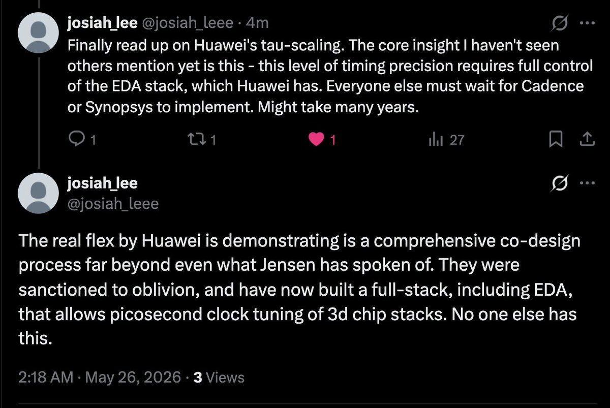
@teortaxesTex Finally read up on Huawei's tau-scaling. The core insight I haven't seen others mention yet is this - this level of timing precision requires full control of the EDA stack, which Huawei has. Everyone else must wait for Cadence or Synopsys to implement. Might take many years.

English
6
4
55
6.1K
Angelica 🌐⚛️🇹🇼🇨🇳🇺🇸
Well…seems like Tau Scaling is a fancy way of saying “we will make the chip a double-decker”. The problem is unlike Moore’s law which lasted for half a century of shrinking transistors becoming more possible you can’t keep getting gains through Tau Scaling. Diminishing returns set in. Eventually for Huawei or any other Chinese semiconductor firm to reach parity with TSMC, they will still need to crack EUV probably. But they’ve gotten remarkably far without it and will get a further still.
fin@fi56622380

华为τ scaling定律营销策略,无非是more than moore的广义摩尔定律的另一种说法而已 作为芯片架构师,我更感兴趣的,还是芯片密度提升,ppt上41%能耗提升和12.7%性能提升,到底是怎么实现的 看完了论文,感觉华为这次创新,本质上是用设计复杂度高 + 高制造成本 + 超前散热,一定程度弥补了工艺差距 ----------------- 1. 华为芯片堆叠带来的等效密度提升,是虚假宣传还是真的,是不是工艺突破?有没有实打实的好处? 等效密度提升的来源,是两片芯片用hybrid bonding技术绑在一起,投影面积理论上能减小一半,但第一代不是全芯片双层折叠,而是选择性折叠关键logic,所以只有大概53%的芯片面积实现了折叠(密度155->238),等到后面几代折叠面积会逐渐增大,到2030年接近全折叠(密度155->292) 这2026第一代等效密度从 2025 年 155 MTr/mm² 跳到 2026 年 238 MTr/mm²,时钟频率也提升了12.7%,功耗比提升41%,表面上看似乎和工艺突破没有什么区别,但有一点重要区别就是leakage power华为从头到尾没有提,只要工艺节点不变,gate leakage、junction leakage 不会因为 3D stacking 自动改善 2030年到2031年的等效密度突变,大概率是来自于2层堆叠到3层堆叠,正如2025到2026年的等效密度突变,时钟频率突变,来自单层到2层折叠 所以从leakage没提这个事来看,这个2031年等效1.4nm,和工艺节点上的突破没有联系。 本质上是用设计复杂度高 + 高成本 + 超前散热 + 超前部署advanced packaging,一定程度弥补了工艺差距 ----------- 那么这样看起来虚假的等效密度提升,有用处吗?好处在哪里? 有的,设计上topology折叠,原来要跑几毫米的水平走线,折叠后变成了几十微米。降低了super buffer/bus的长度,降低了clock tree的深度(clock depth -42%、clock wire -28%),clock skew也带来了改良(-25%),这对动态功耗的改善是实实在在的。部分critical path的缩短,也让时钟频率的上升更容易 所以ppt roadmap上performance的提升,从2025年到2026年上升了12.7%,大部分都是来自于时钟频率的上升(12.7%) 所以好处基本上是topology拆分电路逻辑设计上带来的提升 既然没有实质上的工艺提升,华为芯片堆叠带来等效密度提升的trade off代价在哪里? 三个代价:散热超前发展,设计复杂度高,制造成本变高 最大的代价就是热密度的同步上升,理论上logic on logic都是CPU execution发热最严重的区域,这部分折叠起来相当于功耗密度直接翻倍,但算上41% power efficiency改善,功耗密度仍只比非堆叠方案高40%左右。所以第一代只能对最关键的部分做折叠,大概只占全芯片面积的53%。 所以散热技术也被逼的超前发展,直接上毫米级的MEMS风扇,做micro-cooling fan。 另外的代价就是设计复杂度的变高,critical path的折叠,哪个部分的logic能折叠,折叠之后又会带来从前端到后端的巨大变化要推翻重来 现有的所有EDA工具也不可能支持3D topology,论文自己也承认,full-scale LogicFolding需要全新的3D-native EDA toolchain,把多层stacked dies当作单一连续设计实体处理。哪些logic能折叠、折叠后的inter-die timing closure怎么做,Physical Design(PD)也是难点 制造成本也会更高,被迫超前部署advanced packaging封装,1.5~2um的hybrid bonding + logic on logic都是很有挑战需要显著更高的成本 以前一层wafer做一次光刻;现在两层wafer分别做光刻再bonding,加上hybrid bonding的overlay控制(论文要求<0.5μm)、TSV、KOZ keep-out zone、冗余修复、良率乘法损失,每颗芯片的制造成本和测试成本都要显著上升 -------------------------- 2. Tau scaling这个说法,scaling的到底是什么,这个scaling技术路线是不是一次性的design topology红利?潜力如何?持续进步的空间在哪里? τ Scaling的核心主张是:用时间常数τ替代几何线宽作为全栈优化目标,在器件、电路、芯片、系统四个层级分别压缩特征延迟 公式本身没有任何新物理。"关注瓶颈延迟"是所有架构师都在做的事情。整个行业都知道互联RC是延迟瓶颈,TSMC每一代工艺都在用low-k dielectrics/semi-damascene等手段降RC。把一个众所周知的优化方向包装成"定律"是显然的营销宣传手段,本质是More than Moore的广义摩尔定律的另一种说法 抛开marketing,华为目前所谓RC delay的改善,本质上是芯片堆叠之后,topology距离缩短,让匹配的effective RC都变小,不是RC工艺常数 至于scaling的意思,是能持续发展的一条roadmap。这里的持续改善路径指的是,全芯片堆叠的层数越来越多,从25~30年的2层堆叠,到31年开始的3层堆叠,以后甚至会考虑4层堆叠 第一代折叠技术甚至不是全芯片双层折叠,而是选择性折叠关键logic,所以只有大概53%的芯片面积实现了折叠(密度155->238),等到后面几代折叠面积会逐渐增大,到2030年接近全折叠(密度155->292)。2031年的roadmap之所以会出现一个阶跃,就是因为那是从2层折叠到3层折叠的时间点。 但需要注意的是,这个scaling方法的边际效应是逐渐缩小的,折叠成双层的收益是100%,2->3层的收益就只有50%,如果2035年再从3->4层堆叠,收益就只有33%了 另外随着堆叠层数变高,上面说到的三个挑战,散热,设计复杂度,成本,都是越来越大 --------------------- 3. 华为的芯片堆叠,是不是TSMC/AMD已经有的hybrid bonding技术?华为做到的是cache on logic,cache on cache,还是logic on logic,logic on logic最大的散热问题是怎么解决的? 是已经有的技术没错,但同时也是把现有技术指标做到了领先也是真的,3D堆叠本身不是新技术,TSMC的hybrid bonding量产还是6um,华为论文给出Kirin 2026的hybrid bonding pitch是1.5μm 我在刚刚看到华为的堆叠消息之后,第一反应也是怀疑和AMD的3D V cache类似,它主要把 SRAM cache 叠在 已经有的L3 cache 区域上,通常会避免直接堆在最热的 CPU execution logic 上,就是避免散热问题,毕竟SRAM 的功耗密度和热点特性与high-activity logic 不一样,如果最热的logic on logic堆叠,散热恐怕会碰到困难 但看了更多数据之后,clock buffer -56%、clock depth -42%、clock wire -28%,这些只有在core内部的clock distribution被重构时才可能发生。纯SRAM stacking不会碰core内部的clock tree。另外如果只是cache on cache,大概率是不需要单独MEMS微型风扇额外散热的,证据普遍都指向logic on logic方式 华为这个技术的精妙之处在于,logic on logic 折叠之后热密度并没有翻倍,而是因为topology的好处,能耗下降了30%,这样热密度只上升了40~50% 而第一代没有完全把整个最热的execution logic 100%堆叠起来,论文也明确说selectively applied along key critical paths,只是大概53%有选择性关键路径会堆叠起来,可能颗粒度都没有那么好,只是IP堆叠在IP上,那么热密度上升也许能维持在20%以内 但这条道路继续前行,超前发展的散热就成了必然,现在是MEMS微型毫米级的主动散热风扇,紧贴处理器传导效率高,和华为手机一样,散热堆料特别足,而且技术领先同行。 以后怕是要把HBM7/8的微流道散热技术提前用起来了,毕竟HBM7/8要上24+层堆叠,华为很可能要在提前用上下个世代的散热技术了 ------------------------- 4. 从架构角度来说,最重要的问题,华为41%的power efficiency(能耗比)提升,到底是怎么实现的?为什么AMD的3D V cache没有这么大的提升? 首先确定41%的定义。论文只说"SoC performance-core power efficiency improved by 41%",没有给出benchmark名称、Voltage/Freq点、温度条件、功耗边界。但PPT roadmap上有一个关键线索:ISO-Power Performance的数字,2025年是2.75,2026年是3.1,提升12.7% 这个时钟频率提升12.7%完全一致,可以理解为,同功耗的性能提升是12.7%,绝大部分是时钟频率提升带来的 至于能耗比上优化的猜测是,LogicFolding缩短critical path → 在固定Vdd下Fmax从2.75GHz提升到3.1GHz → 这意味着在原来的2.75GHz频率下,有了约12.7%的timing headroom → 这个空间在iso-performance模式下可以换成更低的Vdd 另外的能耗比的提升,可能也来自于电路折叠之后,cache hit latency的下降。从业界经验来看,一般L2/L3 cache hit latency下降10%,CPU整体性能会有至少5%的提升 ppt里显示SRAM latency下降30%,估计会有一部分转化为cache hit latency的下降 AMD的3D V cache没有这么大的提升,主要是因为AMD的底层logic die并没有重新设计,3D cache的延迟latency不仅没有减小反而加大,只是增加了cache大小,收益不如latency下降那么明显。 另一方面,clock skew的下降,critical路径变短,造成电路timing变好,意味着华为可以使用更低的vdd(猜测甚至能低7~8%),以及路径缩短所带来的RC的下降(考虑到clock buffer -56%、wire -28%、SRAM pJ/bit -24%这些数字,比如C_eff下降10~15%合理),再加上clock tree的整体缩短和下降,确实是有可能在部分Voltage/Freq点做到同性能下,做到30%的功耗下降的,而30%的功耗下降换算过来就是41%的power efficiency 对比苹果和高通,每一代手机芯片在iso-power下单核性能一般提升10-20%,iso-performance下功耗一般降30-40%,这是V/F曲线的特性决定的,所以从经验上来说,数字是对的上的。 所以这个power efficiency(能耗比)的提升,从现有的数字上来说可以从topology推导出来是合理的,可能真的和工艺节点没有太大关系 ---------------------------- 5. 这个技术路线有没有可复制性,其他家会不会效仿? 短期内不会大规模效仿,因为性价比和风险收益比来说不好。长期来看,这个方向所有人都在走,只是名字不一样 华为做LogicFolding的根本驱动力是制裁,工艺节点被卡在7nm,只能在封装,散热,和设计层面想办法弥补。华为也为此付出了不小的代价:散热成本,设计复杂度,以及制造成本更高(包括良率)。这是一个被逼出来的路线,不是一个自然选择 其他玩家在用TSMC就能做到正常的经济迭代,是没有必要冒着这个风险,去超前迭代散热技术和设计复杂度的 长期来看,Intel的Foveros、TSMC的SoIC、AMD的MI300的3D stacking都在朝同一个方向走。如果继续追最先进节点的经济性持续恶化,那么"固定一个成熟节点+3D topology optimization"的路线会越来越有吸引力 散热方面,MEMS微型风扇和微流道也会成为未来HBM散热的主流 ------------------- 总结一下,华为这次的创新,绝对是值得尊重的,在制裁环境下,用极高的设计复杂度和成本,在一个被锁定的工艺节点上大胆重新设计,榨出了一次大的topology红利,虽然它有天花板。每多加一层的边际收益递减(堆叠1->2层, 2->3层, 3->4层,提升百分比变小),leakage无法解决,散热越来越难,3D EDA工具链更是全新的挑战。 但这个Tau scaling不是一条可以走十年的指数增长路径,每次爬完一个台阶,下一个台阶更难爬,而且台阶更矮收益更小,华为以后想缩小差距,还得再想想靠什么其他的路线

English
17
5
69
9.8K
josiah_lee
josiah_lee@josiah_leee·
@teortaxesTex Three main challenges - immersion DUV, stage metrology, and stage speed. It's a hard problem (@lithos_graphein is absolutely right), but depending on who you talk to, they are at 14 or 28nm equivalent right now, and have a 24/7 crash development program to drive it down to SOTA.
English
0
0
9
210
josiah_lee
josiah_lee@josiah_leee·
@teortaxesTex Lol, I guess he needs a new grift, and he senses potential in "India Supapowa 2030". I think it will work quite well, Indians can't resist a white man (well, white enough anyways) telling them they are special kangs whose time will soon come.
English
0
0
5
404
josiah_lee
josiah_lee@josiah_leee·
@joequant The East Asian propensity for gambling and numerology gets one-shotted by technical analysis influencers in a bull-market. It's insane how bad it is. Boomers YOLOing on stock tips from randos drawing lines on candlestick charts. Aunties trading on leverage with no sense of fear.
English
0
0
2
130
Joequant
Joequant@joequant·
Again this is something that is obvious if you are in the neighborhood. My Taiwanese wife and her friends are all playing the stock market. This is going to end very badly, because once the stock market goes up, then everyone tries to make money playing the stock market.
Brad Setser@Brad_Setser

The main counterparts, other than TSMC investment abroad (FDI outflows = ~ $40b) are portfolio equity outflows and bank outflows. Taiwanese investors selling TSMC to diversify? foreign investors lightening up? The bank flows could come from "reverse hedging" by the lifers ...

English
2
1
19
1.9K