
Jason
978 posts
Jason
@Jason94209409
Stochastic Capital Allocator 🤡🫵
Metaverse Katılım Mayıs 2018
1.3K Takip Edilen73 Takipçiler

FYI: I went long on $ARM at $139.
Genuinely a compelling long at $143B MC as markets shift more from training -> inference.
Then $ARM AI CPUs cannibalize the market for inference and $NVDA market share.
Especially as LLMs get more lightweight.
The projections to $25B/revenue (5x revenue) are already insane to justify risk-reward.

Serenity@aleabitoreddit
$ARM expects $15B in annual revenue from the the AGI CPU: "The company projects that the new chip business will generate over $15 billion in annual revenue" within the next 5 years. 5 times current revenues (~$25B revenue)... Arm probably deserves to be up more than 5% on this news if they're multiplying their revenue with a new product overnight?
English


MiroFish runs 1,000,000 AI agents to simulate how a future event plays out
> Upload news
> Agents debate & form coalitions
> A probability map of outcomes emerge
1M runs. Happened 3200 times. p ≈ 0.32
The most powerful forecasting tool is open source
English

JUST IN: Billionaire Stanley Druckenmiller says the global payment system will run on crypto stablecoins within 15 years because they are more efficient.

English

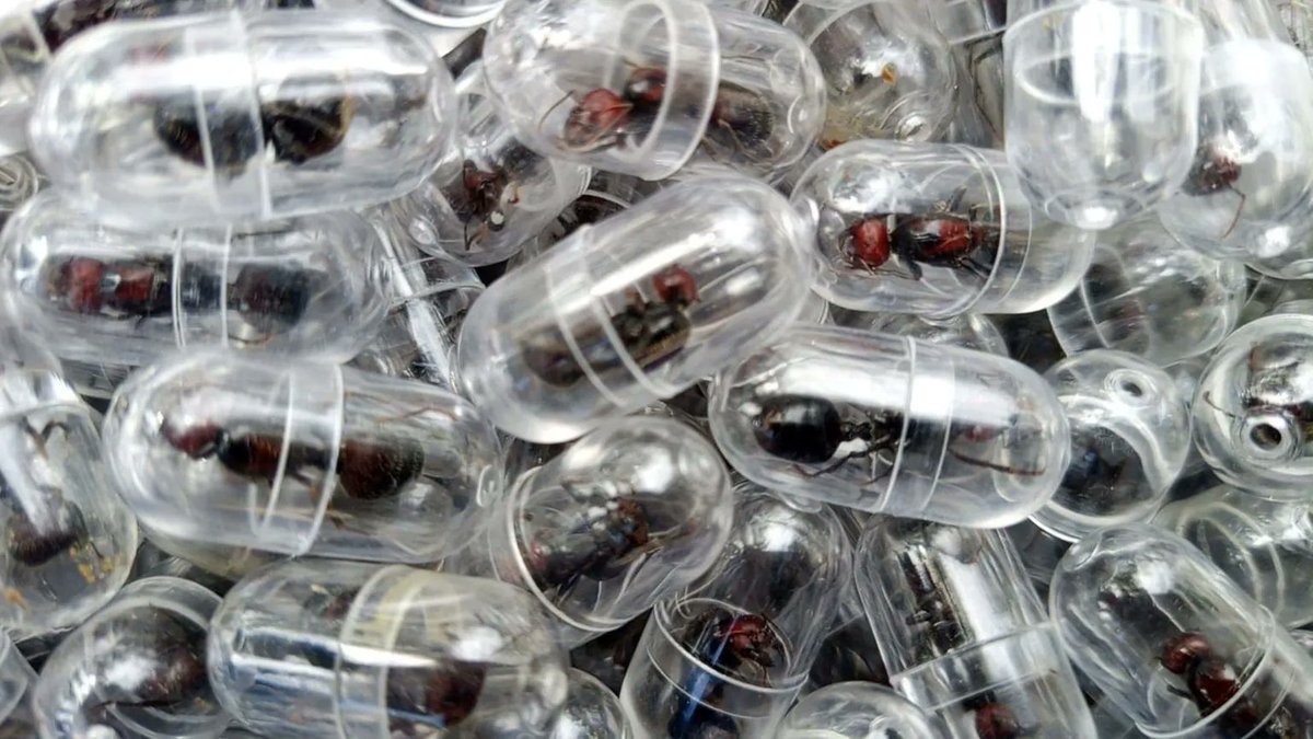
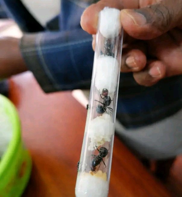
A Chinese citizen has been arrested for attempting to smuggle 2,000 queen ants out of Kenya 🇰🇪. 🐜🚨
English
@crux_capital_ @grok which one of these captures the largest value in the photonics supply chain ?
English

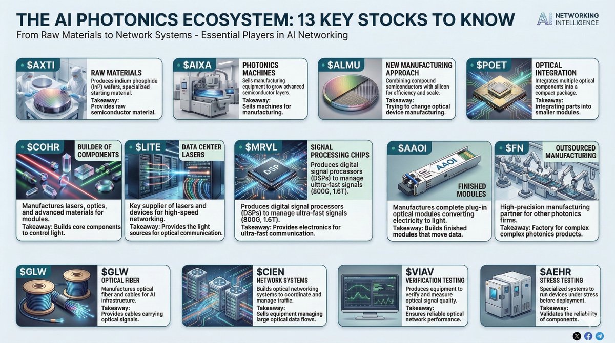
Education Saturday! ✍️
If you're new to Photonics, start here!
$POET $LITE $COHR $AXTI $AAOI
Here is a really easy and simplified way to understand many of the companies that I track in this space
Save/share if you found this useful please!
$AXTI - The raw materials
AXT produces indium phosphide (InP) wafers, which are specialized semiconductor materials used to build lasers and photodetectors.
Think of these wafers as the starting material used to make many of the optical components used in AI networking.
$AIXA (honorable international mention) - The machines that make photonics possible
Aixtron sells the manufacturing equipment used to grow the advanced semiconductor layers that form lasers and detectors.
These tools are used by companies that actually manufacture optical components.
$COHR - A major builder of optical components
Coherent manufactures a wide range of photonics products including lasers, optics, and advanced materials.
Their components are used inside the optical modules that carry data between servers in AI data centers.
$LITE - A key supplier of lasers for data centers
Lumentum focuses heavily on lasers and optical devices used in data center networking.
These lasers are what actually generate the light signals that travel through optical fiber.
$ALMU - A new approach to building photonics
Aeluma is working on a different way to manufacture photonic devices by combining compound semiconductors with large silicon wafers.
The goal is to produce lasers and detectors more efficiently and at larger scale.
$POET - Shrinking multiple optical parts into one
POET develops technology that allows multiple optical components (like lasers and detectors) to be combined into a compact integrated package.
This can simplify the design of optical modules used in data centers.
$MRVL - The chips that make the signals usable
Marvell produces digital signal processors (DSPs) used inside optical transceivers.
These chips clean up and manage the signal so data can travel at extremely high speeds like 800G or 1.6T.
$AAOI - The finished optical modules
Applied Optoelectronics manufactures complete optical transceivers.
These are the plug-in modules that sit inside switches and servers and convert electrical data into light, then back again.
$FN - The factory for many photonics companies
Fabrinet specializes in building complex optical products for other companies.
Many photonics firms design the technology but rely on FN to manufacture it at scale.
$GLW - The fiber that carries the light
Corning manufactures optical fiber and fiber cables.
These fibers are the physical paths that light travels through inside and between data centers.
$CIEN - The systems that run the network
Ciena builds large-scale optical networking systems used to move data across data centers, cities, and long-distance networks.
Their equipment coordinates and manages enormous flows of optical traffic.
$VIAV - Testing that everything works
Viavi produces testing equipment used to measure optical signals and verify network performance.
These tools are used by manufacturers and network operators.
$AEHR - Stress testing the components
Aehr makes specialized test systems used to run semiconductor and photonics devices under extreme conditions before they ship.
This helps ensure the parts will operate reliably inside data centers.
...
These are simple ways to think about these companies. Obviously they have lots of product mix and exposure to different areas, so just use this as a really simplified way to think about each company!
Also, yes there are many many good international players. I just don't cover them.
Gaetano@crux_capital_
Education Saturday! 📓 For all my Photonics followers, you'll want to learn this $AXTI $LITE $COHR $GLW $POET etc. The Photonics Supply Chain: Start to Finish. Step 0: Mining and Refining It starts with a metal called indium. Indium is what makes high-performance data center lasers possible today. Without it, you can't build the components that move data at the speeds AI demands. Indium has no dedicated mines. It doesn't get extracted on its own. It's a byproduct of zinc refining, meaning it only gets recovered when zinc smelters have the equipment and economic incentive to capture it from their waste. Step 1: The Substrate Refined indium gets combined with phosphorus to create a material called Indium Phosphide, or InP. InP has a unique property in that it can generate light directly from electricity. Silicon, the material that runs everything else in computing, cannot do this. That's why InP is the go to for the lasers inside data center optical components. The first thing you make with InP is a wafer which is a thin, flat disc that serves as the foundation for everything built on top of it. InP wafers are expensive, brittle, and difficult to produce at large sizes. The industry is only now moving to 6-inch wafers. For context, standard silicon chip fabs run on 12-inch wafers. That size gap is a big part of why photonics capacity is so hard to scale quickly. Step 2: Epitaxial Growth A bare InP wafer still can't do anything useful. To create a laser, you have to grow extremely thin additional layers on top of it, each just a few nanometers thick (a human hair is roughly 80,000 nanometers wide). This process is called epitaxy. The exact chemical composition of each layer determines the laser's wavelength, power, and efficiency. Get it slightly wrong and the entire wafer is scrapped. This step requires specialized equipment found in very few places in the world. It's rarely talked about, but it's one of the most critical bottlenecks in the entire supply chain. Step 3: Wafer Fabrication Now the actual circuit gets built. Using techniques similar to semiconductor chip manufacturing (patterning, etching, depositing materials etc.) engineers carve microscopic structures into the wafer: the channels that guide light (called waveguides), the cavities where light gets amplified, and the components that switch it on and off. Unlike standard chip manufacturing, at this time this cannot be done in a regular semiconductor fab. It requires a dedicated photonics facility. These take years to build, qualify, and ramp. There are very few of them in the world. Step 4: Dicing and Yield The finished wafer gets cut into individual chips. Each chip is then tested to see if it actually works to spec. The percentage that pass is called yield and it's one of the most important numbers in this business. Low yield means high cost per working chip. Improving yield is one of the biggest levers on profitability, and it's hard-won through years of process refinement. You probably won't see it reported directly, but it's hiding inside gross margins. Step 5: Component Assembly A working laser chip still can't be used on its own. It has to be physically aligned to an optical fiber with tolerances finer than a fraction of a micron and combined with other components like light detectors and signal modulators to create a functional optical sub-assembly. Automating it reliably at high volume remains one of the hardest manufacturing problems in the industry. The assembled component also has to be hermetically sealed inside a protective ceramic and metal enclosure. Data centers run hot, and moisture or dust will degrade a laser chip quickly. These hermetic packages are specialty components with few suppliers and long lead times and they have shown up as a bottleneck alongside InP when demand spikes. Step 6: The Transceiver Module The optical sub-assembly goes into a housing along with a DSP chip (a processor that cleans up and interprets the light-based signals) plus a circuit board and casing. The result is a pluggable transceiver: the finished module that slots into a switch or server in a data center. These individually get tested before it ships. That testing process is slow and expensive, and it's a hidden constraint on how fast output can actually scale. Note, in the world of CPO this will change. Step 7: Into the Data Center It plugs into a port on a network switch inside the data center, the hardware that routes data between thousands of servers. And none of it moves an inch without the fiber it runs through. Ultra-pure glass strands, thinner than a human hair, carrying light signals between every switch, server, and building. Follow stocks in this space? Drop a ticker below and I'll tell you exactly where they sit in the stack 👇
English
@hamptonism So basically non-technical autistic interns are controlling the price of BTC 🤣
English


How I'm positioned:
Long memory/Korea/Claude (but watching for exit signs)
Getting more long bonds
Still long defense (but less than before)
Still long LatAm and $ORR
Getting more long industrials
Thinking about how much China is optimal to own here.
English
@StockMarketNerd @Brian_Stoffel_ Oracle of Omaha > SPAC-oil Salesman
Indonesia

Buffett > Chamath
Not particularly close either.
English


Be me, Dutch investor
Netherlands approved 36% unrealized gains tax
WTF does that even mean
Put $1,000 into stocks
Year 1:
• Stock goes to $2,000
• Government: "you made $1,000, pay $360 cash tax"
• MFW I didn't sell anything
• Forced to sell shares to pay
• Everyone else forced to sell too
• Mass panic selling
• Stock crashes to $800
• I have $440 left after paying tax
Year 2:
• Stock recovers to $1,200
• Government: "you made $400, pay $144"
• Forced selling again
• Price drops to $900
• I have $756 left
Year 3:
• Stock at $1,000
• Government: "you made $100, pay $36"
• Smart money has fled Netherlands
• I have $964 in stock
• MFW I paid $540 in taxes
• MFW stock is back where it started (0% gain)
• MFW I only have $460 left
• Lost 54% on a stock that broke even
MFW the government made more money off my investment than I did
Government: "Thanks for the $540! 😊"

The Kobeissi Letter@KobeissiLetter
BREAKING: Netherlands’ House of Representatives has approved a 36% tax on unrealized capital gains.
English

the following is generated using an ensemble model, ie prompting chatgpt gemini claude using their most advanced models and deep research about ~10 times, then averaging the 10 results using a reasoning model.
—
The 10 most AI-durable competitive moats in the world
1. TSMC — Controls 90% of cutting-edge AI chip fabrication with $30B+ per fab costs creating insurmountable barriers. AI demand is tripling revenues while geopolitical risk in Taiwan remains the key concern.
2. Visa — 300B+ annual transactions across 200+ countries create an unbreakable two-sided network built over decades. AI agents needing trusted payment rails make Visa more essential, with agentic commerce growing ~45% CAGR through 2030.
3. ASML — 100% monopoly on EUV lithography — the only machines that can make advanced AI chips, with China’s alternative 15-20 years behind. Pat Dorsey’s #2 holding at 15% of portfolio; export controls to China are the primary risk.
4. MSCI — Indices benchmarked to $15T+ in global assets, embedded in regulatory frameworks and ETF structures, making them “effectively irreplaceable.” 80%+ gross margins with AI raising rather than lowering competitive barriers for would-be disruptors.
5. S&P Global — Duopoly in credit ratings reinforced by SEC regulation, with $15.3B revenue and 50% operating margins. $1B+ invested in AI since 2018, though the stock dropped 18% in one day during the Feb 2026 SaaSpocalypse on conservative guidance.
6. Moody’s — Shares the regulatory-embedded credit rating duopoly with S&P, with ratings potentially even more resilient due to deeper regulatory entrenchment. The Orbis private company database is a unique proprietary data asset that AI makes more valuable.
7. Mastercard — Mirrors Visa’s network moat across 210+ countries with $7B+ invested in cybersecurity and AI. Launched “Agent Pay” for AI agent transactions, transforming transaction data into high-margin analytics.
8. Microsoft — 350M+ commercial Office 365 users, Azure growing 40%, and a $10B AI inference run rate — the fastest revenue ramp in business history. Enterprise switching costs make replacement “open-heart surgery,” but $80-93B in capex with uncertain returns is the risk.
9. Alphabet/Google — 16.4B daily searches generate the world’s richest intent dataset, while YouTube provides unmatched multimodal training data. AI Overview monetizes at parity with traditional ads, though search share dipped below 90% for the first time since 2015.
10. Hermès — Possibly the most AI-proof moat on Earth: 187 years of heritage, hand-stitched Birkin bags, and artificial scarcity that no algorithm can replicate. Overtook LVMH as Europe’s most valuable luxury company, but trades at 52x earnings — 56% above Morningstar’s fair value.
English


@jon_charb Hyper liquid is in most respects everything wrong with crypto
Founder literally fled his home country to build
Openly facilitates crime and terror
Closed source
Permissioned
English

absolutely elite research
HIP-3 Silver perps are delivering tighter spreads & better execution for retail than CME/COMEX Micro Silver futures, and Hyperliquid is open 24/7
imagine being bearish crypto when we're just starting to beat tradfi at their own game
Hyperliquid
shaunda devens@shaundadevens
English


THIS IS IT.
I’m officially 95% out of the market.
S&P 500 price now: 6,983
I’ve been in this game for more than 20 years.
Here’s why I decided to get out:
First of all, didn’t sell my long term BTC stack I’ve been holding since 2013-2015, my metals and real estate.
Does that mean the market will crash tomorrow?
NO. ABSOLUTELY NOT.
I’m not a day trader.
But there’s a good chance we’re very close to a market top and could drop 15–20% from here.
The smartest founders in history are all rushing to the exit at the same time.
– SpaceX
– OpenAI
– Databricks
– Anthropic
They’re aggressively targeting 2026 IPOs with a combined $4T valuation.
They aren’t selling because they need cash.
They’re selling because they’ve identified the top.
We’ve seen this exact setup twice before.
The 2000 Dotcom crash and the 2021 SPAC mania.
Insiders use the window to distribute shares at unsupportable valuations (100x revenue).
The math ain’t mathing.
Big Tech are burning a shit ton of money trying to chase the AI narrative.
– $400B in AI Capex
– Only ~$20B in revenue return
To justify this spend, they need $2 Trillion in new revenue by 2030.
That isn't an investment. That’s a bubble.
And look who else is leaving.
Warren Buffett is sitting on a $300B+ pile of cash.
He’s been aggressively selling into this rally.
He doesn’t want to buy the dip.
He wants to survive the crash.
Then there’s the 2026 debt wall.
Zombie companies survived on 0% interest rates, but now the bill is due.
They have to refinance BILLIONS this year at significantly higher rates.
Most won't survive it.
Let’s see how this plays out.
Keep in mind: I called the last 3 major market top and bottom publicly.
When I start buying again, I’ll say it here for everyone to see.
Many people will regret not following me sooner.
English


I have just been informed that one of the teams competing in the AI Grand Prix is using a biological computer built with cultured mouse brain cells to control their drone.
At first look, this seems against the spirit of the software-only rules. On second thought, hell yeah.
English