@OnodaCapital Orbital doesn't work until you figure out 400 ft radiator mass
English
Elapsus
179 posts


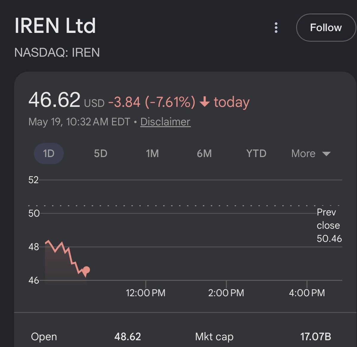

I still am bearish on $IREN. Algorithms/retail probably read $NVDA + $IREN partnership and bought it up. However, if you look at the realtity, it's just looks like brand agreement giving $NVDA risk-free convertible notes. So $IREN can continue selling their $6,000,000,000 ATM into retail investors. It's the equivalent of a startup using AWS and saying they have an Amazon partnership so give them $6B. This wasn't Nvidia directly funding $IREN yet, just a risk free option to. There's a "5 GW deployment" but I'd rather not be the one buying into the dilution to fund it.


TSMC 2026 Technology Symposium (Taiwan 5/14) Summary: Global Expansion & Operations · Global Build-out: Constructing or modifying 18 fabs worldwide (includes 5 advanced packaging plants). · Taiwan Core: 12 of these 18 facilities are located in Taiwan. · Acceleration: Expansion speed has doubled to 9 new plants per year (2025–2026) vs. 4 per year (2017–2024). International Site Progress · Arizona (USA): -Fab 1 output to grow 1.8x in 2026. -Fab 2 equipment move-in 2H-2026 (N3 production 2H-2027). -Fab 3 broke ground 1H-2025. -Fab 4 and first advanced packaging plant (AP1) are in initial construction. · Kumamoto (Japan): -Fab 1 (28/22nm) yield already equals Taiwan levels; 2026 output target is 2.3x YoY. -Fab 2 began construction in 2025 for N3 production. · Dresden (Germany): -ESMC facility focusing on 12nm–28nm for Automotive/Industrial. Advanced Process Roadmap (N2 / A14 / A12) · N2 Momentum: Fab 20 (Hsinchu) and Fab 22 (Kaohsiung) are in mass production. Taichung Fab 25 to follow in 2028. · N2 Performance: First-year output expected to be 45% higher than N3's first year. Capacity expansion CAGR of 70% seen 2026–2028. · Yield Maturity: N2 yield learning curve is 2 quarters ahead of N3 at the same stage, driven by AI-optimized manufacturing. · A14 (1.4nm): Already achieved >80% yield on 256Mb SRAM; offers 10–15% speed boost or 25–30% power reduction vs. N2. · New Nodes: -A12 (Performance-focused with Backside Power/Super Power Rail) and A13 both targeting 2029 production. -N2U(enhanced 2nm) slated for 2028. · Next-Gen: CFET architecture reduces SRAM cell area by 30%vs. Nanosheet. Advanced Packaging & Silicon Photonics · CoWoS Scale: 5.5x reticle size now at 98% yield. Scaling to 14x reticle for 20 HBMs by 2028 and 24 HBMs by 2029. · System on Wafer (SoW): Future "Super Exchange" chips to integrate 64 HBMs/16 CoWoS units, exceeding 40x reticle size with 100TB+ bandwidth. · Growth: 3DIC/CoWoS capacity CAGR of >80% 2022–2027. · COUPE: All-optical interconnects to replace copper as data centers scale to millions of GPUs and power needs surge 200x. Specialty & Memory Shift · The Memory Divorce: Shifting from eFlash to RRAM (ReRAM) and MRAM for advanced nodes (≤28nm) in Auto, AI Glasses, and Edge AI. · Edge AI Specs: -N4PRF (RF process) for 39% power reduction -N16HV(16nm High Voltage) specifically for AI Smart Glasses/AR displays. $TSM $NVDA $AAPL $AMD $AVGO $MRVL $INTC $AMZN $GOOGL $MSFT $META #semiconductors Links: news.cnyes.com/news/id/6458515 cna.com.tw/news/afe/20260… ctee.com.tw/news/202605147… money.udn.com/money/story/56…