

1
28 posts


对吧,说了见底了,坚定相信多头就行了
接下来的行情可能比2-6月的行情还炸裂,账户3-5倍都可能,因为筹码被gjd归集了,你要知道他们归集核心科技的那么多筹码,最后是为了完成什么任务...
Elias Vance@EliasVanceQuant
我搞了点光模块,天孚和东山。 反弹快的话今天中午,慢的话明天开始。
中文

又一组数据出炉,印证了我所说的,制造业回流美国的幻想已经破灭了,贸易逆差继续扩大,进口不断扩大,出口连续下滑。现在叙事上说的是加息预期,但市场已经偷偷交易另一个逻辑了,就是美联储嘴炮。股市已经在交易早期滞胀了,债市的传导在早期,收益率又不知不觉到了历史高位。这种传导不是匀速累积的。而是我们会看到初期传导迹象,先是一点一点的,然后突然爆炸。
x.com/i/spaces/1qgvv…
中文
这几天一直在说缩圈行情难做,买错方向的还是会巨亏。
自己看吧,今天以为磷化铟很强是吧?追高买进去有研新材日内就能巨亏-10%,明天还要计提。要是跟买了中船特气的已经赚回来一半亏损了,更别提现在水下还有几只很有爆发动能的潜力股🤣
中文

This article is fully open to everyone.
In this piece, I cover two things.
First, for readers without a technical background, I explain how NVIDIA rack names are structured and what each part means.
Second, based on that foundation, I analyze SemiAnalysis’s July 6 post. I go through what it implies, why those posts may sound alarming, and what the actual midplane yield picture could look like in detail.
The first part is written for readers who may not have a technical background. If you only want to read my thoughts on the latest @SemiAnalysis_ post, please jump directly to Section 5.
Damnang@damnang2
English

This is a fantastic post! I'm going to have to re-read later to deeply process.
At first glance, this explains why Qualcomm's HBC might actually work out great for inference without CoWoS or HBM... they just have to get the 3D stacking right.
Interconnect is everything. Start with that.
Optimize for latency, not memory bandwidth.
Design inward towards compute from there.
Lots of untapped potential still in AI hardware.
Big Boss@0xBADB01E
I agree with this post whole heartedly but I’d push it even further. The interconnect IS the binding constraint for AI even more so than memory. If we want faster inference & training with better economics we are best served by designing our interconnect first and then working backwards towards the optimal chip architecture. Today’s chips weren’t really designed with this principle in mind. There is no better example than running autoregressive decode on a GPU. Despite all those reticle sized logic dies & CoWoS integration decode runs at under 20% of peak FLOPs on Blackwell, wasting silicon and burning power while waiting for memory. The naive solution has always been to increase memory bandwidth whether that’s adding more HBM or using SRAM. However, that is a vast simplification of the problem which I’ll explain later. But if you were clever you’d have realized while reading that you could feed those idle FLOPs by streaming weights over the interconnect itself. Wallah 🪄 you just discovered the idea that forms the basis behind disaggregated memory from first principles. But sadly this currently doesn’t work on Nvidia’s hardware. NVLink5 carries 1.8 TB/s against 8 TB/s of local HBM, and scale out is 80x behind that. The “pipe” is smaller than the memory at the other end and thus leads to worst token/sec if its relied upon. But we get an interesting lemma out of this which is that remote memory is only as fast as the interconnect. Therefore you must balance the pipe for the memory it attaches to. SRAM needs an 80 TB/s link, HBM needs 2+ TB/s, and LPDDR gets away with a couple hundred GB/s. So Nvidia selling a rack of 72 GPUs, each GPU’s memory is pretty segregated. The core idea is still sound though but this raises a question, why would Nvidia build a fabric that’s high bandwidth and high latency leading to memory access being segregated per GPU? It’s because they were optimizing for training over inference. Training is dominated by collectives on huge tensors, and a couple microseconds of latency on a huge all reduce operation is just noise so the bandwidth gains justify the latency tradeoff. But more importantly, this also works because it matches what the chip is good at. GPUs are great at hiding latency with occupancy (also what allows them to be OK for training) but bandwidth is the only thing warp switching can’t create. You can justify a 224G PAM4 + FEC with overhead when you have a chip that’s designed to be latency tolerant as well. It’s a latency tolerant fabric for a latency tolerant chip. Maybe a good design for training but inference inverts this completely. Now everyone knows decode is bandwidth bound so you might assume again that more/higher BW memory and thus higher BW interconnects are necessary. However, it’s the exact opposite and the name of the game is actually lower latency and that’s why despite having high bandwidth memory MFU on decode is still so low and also why I made the point earlier that the interconnect is MORE important than the memory itself as well as the chip architecture. In part two I will explain why lower latency interconnects are not just ideal for inference but also allow you to get away with a smaller cheaper memory and a simpler chip architecture.
English

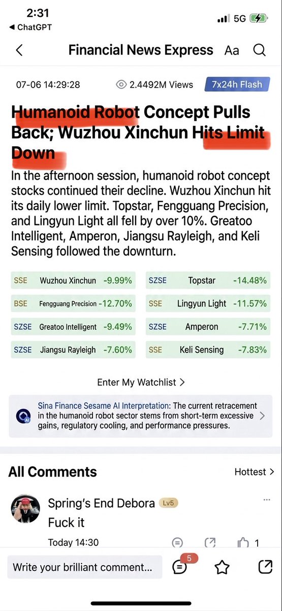
Just as Liwei suggested last Friday. that humanoid robot stocks might be nearing their peak.
Today the Chinese humanoid robot names all crashed to limit down.
There's still time to get out of US humanoids stocks😬
Liwei上週就跟你們說人型機器人相關類股要逃跑了吧!中國人型機器人相關類股今天都跌停,美股應該還有機會逃吧?
$CCXI $VPG $OUST

LIWEI_TW Capital@LIWEI_TWCapital
Liwei’s prediction: The humanoids robot trade will start fading next week. Capital rotates back to the real story: AI infrastructure buildout. If you’re still chasing robot stocks… it might be time to get out. The theme is simply too early. And after seeing the latest humanoid robot from UBTECH, I honestly had nightmares. Maybe it’s better if this technology develops a little more slowly. 😂 youtu.be/NvDFvtMqtzM?si…
English
@babyfolio @kverdek 赞同你的观点,严格来说,这篇报告 CPO 的延后应该是对可插拔的光模块的利好,延长周期,并且对 NPO 的技术路线上升一个新的讨论度,行业重新开始审视良率,但还是会跟你说的一样 市场会一篮子打包出售
中文

Another bearish CPO hit piece.
What do I think of it?
If true, it's bearish $AAOI $LITE $COHR $SIVE
SemiAnalysis@SemiAnalysis_
MASSIVE DELAY: Just 3 months after Jensen demoed Kyber NVL144 at GTC, it has faced major setbacks and has been delayed by more than 12 months, pushing it back to 2028. Below, we explain why Kyber has faced massive delays and why NVIDIA’s NVL72x2 back-to-back rack architecture was also cancelled, leaving Rubin Ultra with a limited scale-up domain. 👇️ 1/6🧵
English
@BitInsighter 您的意思我大概明白了,也就是说,这个资源会向更可能占领市场的那方倾斜,去优化整个市场的结构、资源调配 ;而 Meta 新业务的发展需求会以另外一种形式重新反哺整个产业链吗
中文
@BitInsighter 您好,我看到您之前有在说内存接口芯片,我自己也在很早有关注内存接口芯片,但是实在不明白它的爆发量级是什么,之前我也向您提问过,想向您再问一下,内存接口芯片在全年会有一个明显的量价齐升吗,或者说它实际在整轮周期里面地位是怎么样的
中文
@aleabitoreddit 您好 我想向您请教一下关于 Meta 的事情,昨晚 Meta 要出租多余算力的新闻,不会是算力冗余,如果 Meta 转向算力租赁云服务的话呢,相反来说应该是更利好整个产业链的发展吧?我这样的理解正确吗
中文

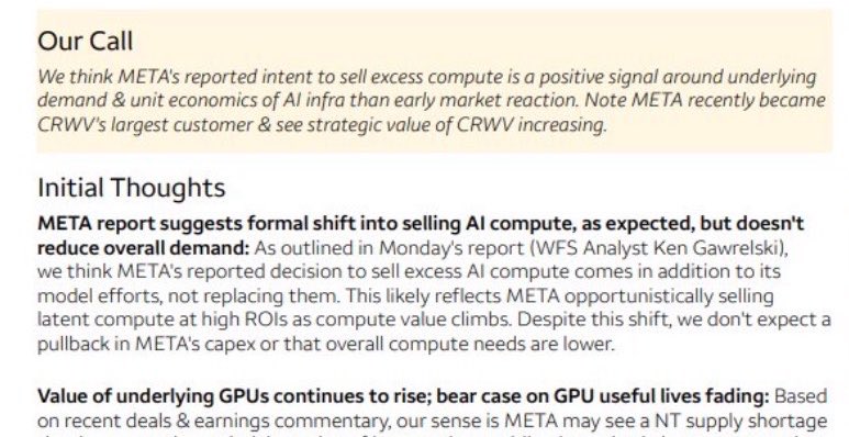
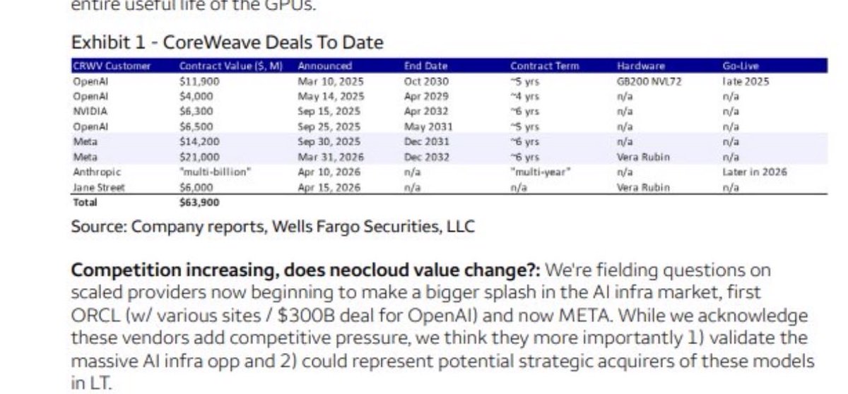
Wells Fargo: $META intent to sell excess compute is a positive signal around underlying demand and unit economics of AI.
“Despite this shift, we don’t expect a pullback in Meta’s capex or that overall compute needs are lower”
Regarding Neoclouds: WF thinks it validated the massive AI infra opportunity as well as acquisition opportunities. Despite any potential competition for Neoclouds.
I’m inclined to agree with Wells Fargo here and say markets completely misunderstood Meta’s excess compute comment.
English

•Lower specs should boost server unit shipments (mild QoQ in 2Q-3Q, strong 20-30% in 4Q26)
•~10% cost reduction on VR200 NVL72 BOM by lowering LPDDR5X capacity, despite memory px hike.
👀👀
Jeff Pu@sssjeffpu
Abstract of “Supply Chain Taking Actions to Manage Memory Cost” •On June 4, news reported that Nvidia VR200 NVL72 cutting default SOCAMM to 96GB modules → CPU-side LPDDR5X drops from ~54-55TB to ~28TB per rack •Vera CPU rack expected to follow by 96GB SOCAMM or 768GB per CPU •General servers shifting to ~50% lower DDR5 spec per CPU based mainly on 96GB/64GB modules •Lower specs should boost server unit shipments (mild QoQ in 2Q-3Q, strong 20-30% in 4Q26) •~10% cost reduction on VR200 NVL72 BOM by lowering LPDDR5X capacity, despite memory px hike. Recommendations: •General servers volume plays, CPUs, CXL, NAND’s XL-Flash/Z-NAND #memory #dram
English

Memory+Compute+Networking is 80% of total CAPEX (China has no advantage here)
The rest 20% is power+cooling+shell
Assuming China is 50% cheaper compared to US
The max net savings is 10%
Teortaxes▶️ (DeepSeek 推特🐋铁粉 2023 – ∞)@teortaxesTex
fun with mafs but the actual reality is that a dollar goes *further* in the US. Models are more powerful, chips do more per watt and second and $, more data has already been collected, labs are larger, older. All other inefficiencies return us to roughly the raw value gap.
English