iFred

25.3K posts

iFred banner
iFred

iFred

@iFred

Semiconductor reply guy analyst.

Seattladelphia Katılım Mart 2008
477 Takip Edilen229 Takipçiler
iFred retweetledi
derek guy
derek guy@dieworkwear·
RIP Sonny Rollins, a great jazz talent and the last surviving musician in one of the best photos of men in suits during the 20th century
derek guy tweet media
English
33
493
3.9K
79.6K
iFred
iFred@iFred·
@CRUDEOIL231 Let them accelerate this nonsense until early July! Those Louisiana salt domes are going to collapse in on themselves and diesel will be 12 dollars a gallon.
English
0
0
0
157
JH
JH@CRUDEOIL231·
They're all screaming peace is here and the SoH is completely unlocked. But when you actually run the numbers for the 24th on Kpler, Vortexa, Windward, and S&P Global, not one of them logs more than 5 tankers crossing. What kind of complete and utter circus is this? Is this another literal replay of March 23rd and April 17th? #oott #iran
English
44
96
895
67.5K
iFred
iFred@iFred·
Copper bump pitches!
Jukan@jukan05

Samsung Electronics Achieves World's First "900-Layer V-NAND"… Countdown to the 1,000-Layer Era Samsung Electronics has become the world's first to successfully implement a prototype of 900-layer-class V-NAND technology, taking another step toward the era of "1,000-layer NAND." Amid intensifying layer-count competition with rivals, the achievement is being seen as Samsung securing a decisive technological lead in a single leap. According to the semiconductor industry on the 25th, Samsung recently realized an integrated 900-layer-class V-NAND system using "Cell Multi Bonding (CMB)" technology, which joins two 450-layer cell wafers into one. NAND flash, which stores data, is a core component in AI servers, smartphones, and data center storage (SSDs). Much like stacking floors in an apartment building, the higher the layer count, the more capacity can be packed into a limited chip footprint, allowing more data to be stored while maximizing power efficiency. It is regarded as a key technology for winning dominance in the AI server and on-device AI markets, where high-capacity, high-efficiency components are essential. In the current mass-production market, SK hynix holds the highest layer count with its 321-layer 4D NAND. However, Samsung—while preparing for mass production of its 10th-generation V-NAND (V10, 400+ layers) this year—has at the same time vaulted to the 900-layer mark at the research stage, positioning itself advantageously in the next-generation NAND market. Regarding these research results, Samsung stated that "normal cell operation characteristics were verified," emphasizing that this goes beyond mere theoretical stacking to demonstrate a level of capability that actually functions. Since commercializing 3D V-NAND for the first time in the world in 2013, Samsung has continuously evolved its processes to overcome stacking limits. In the past, it used a "single-stack" method of drilling and stacking fine holes in a single pass, but as layer counts rose, it ran into physical limitations such as wafer warpage and alignment errors. In implementing the 900-layer device, Samsung resolved wafer warpage—the biggest obstacle—by adopting an advanced upper chuck design. Misalignment errors that occur during bonding were overcome with its proprietary "new overlay correction" technology. Newly introduced bitline (BL) and wordline (WL) structures also delivered meaningful gains, simultaneously reducing power consumption and chip size. Globally, China—led by Yangtze Memory (YMTC)—is chasing Korean firms at the threshold of 300-layer-class NAND mass production. With government support and the localization of equipment, it is pursuing capacity expansion and technological advancement at the same time. If YMTC succeeds in mass-producing 300-plus layers within the year, price competition could intensify and pressure Korean firms' profitability. For this reason, Samsung's 900-layer achievement is highly regarded as a strategic move to build a technological barrier over the medium-to-long term. An industry official said, "900-layer NAND technology is not simply three times 300 layers—it is a technology that changes the paradigm of the stacking process," adding, "It sends global customers the message that Samsung remains the technology leader, and it will have the effect of limiting Chinese firms' volume and price offensive."


English
0
0
0
68
iFred
iFred@iFred·
@scottfutile @NormalIslandNws I’ve just received word that not only does Scott Andrews have nuclear material in his home, but he is actively coordinating with Hamas to bring that material to Israel. @IDF and @IsraeliPM please confirm Scott isn’t a threat.
English
1
0
36
357
iFred
iFred@iFred·
@Aaronwei3n This has been a science experiment since early 2024. So much of this was built around the idea that there would be a tsunami of DDR4 from other YAWNS but the current market may have changed that.
English
0
0
2
230
Aaron
Aaron@Aaronwei3n·
Hearing some chatter about $GOOGL potentially still pushing forward with a standalone DRAM rack. Has anyone in the supply chain caught wind of this recently, or is it just noise? Would be a fascinating push toward true memory disaggregation if true.
English
6
2
41
10.6K
iFred
iFred@iFred·
@zephyr_z9 @dnystedt Was thinking about heat dissipation but it’s a low voltage chip and the CTE is negated due to physical size and material.
English
2
0
0
225
Dan Nystedt
Dan Nystedt@dnystedt·
Big claims, but no major technical breakthrough detailed here. Great marketing and a warning to TSMC, Samsung to make sure Huawei hasn't tricked them into manufacturing advanced chips again. $TSM $SSNLF
Huawei@Huawei

HUAWEI has presented the Tau (τ) Scaling Law, a new principle for guiding the future development of the semiconductor industry. By 2031, HUAWEI's high-end chips based on this law are expected to feature a transistor density that is equivalent to 14 Å (1.4 nm) processes.

English
17
13
171
34.2K
🏴‍☠️
🏴‍☠️@calvinfroedge·
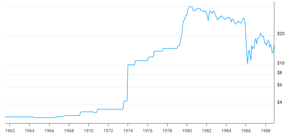
Oil didn't even go up violently in the 1970s until it did Just a little bit at a time, and then suddenly it quadrupled Then it doubled again And before you knew it had done a 10x in less than a decade People get caught in the news flow and lose the big picture
🏴‍☠️ tweet media
English
38
73
826
40.3K
iFred
iFred@iFred·
@CRUDEOIL231 Have you not considered that Barak has a family to feed? You can’t tell me you wouldn’t become the prolapsed anus of the administration, letting slimy ribbons of well timed “news” drip from your protruded and puckered mouth.
English
0
0
0
370
iFred retweetledi
포시포시
포시포시@harukaze5719·
Tbh, I think covering the capacity by expanding the CPU's DRAM and CXL is a more realistic solution than HBF. The more I look at HBF and NAND, the more my skepticism is reinforced because their fundamental origins are different from DRAM...
English
2
3
26
3.1K
iFred
iFred@iFred·
@zephyr_z9 There are some serious science projects at gChips. The HBF designs that I’ve seen over the past few years just look like socketed NAND on the accelerator or in pooled setups. I think a lot of tourists are getting hung up looking for the next big thing.
English
1
0
3
388
Zephyr
Zephyr@zephyr_z9·
@iFred There are rumors of Google adopting it Nvidia isn't interested rn, so companies are not taking its development seriously for now
English
1
0
8
875
Zephyr
Zephyr@zephyr_z9·
Yup, using HBF for GIDS doesn't even make sense HBF won't be used for any write-heavy tasks like KV cache storage (as it will kill the NAND in 2 years) You can use it for storing weights If it's ever adopted, the structure will be something like 8 HBM stacks + 4 HBF stacks "NVIDIA is looking to use high-reliability, high-speed NAND, such as 200M IOPS NAND, for GIDS. It is not considering HBF."
Jukan@jukan05

The report claiming that NVIDIA is using HBF is fake news. I’m extremely disappointed in TrendForce. For a reputable firm like TrendForce to cite a The Elec article that was based on one professor’s opinion, and then reinterpret it as if The Elec reported that NVIDIA is trying to use HBF, is simply unacceptable. This is not true at all. NVIDIA is looking to use high-reliability, high-speed NAND, such as 200M IOPS NAND, for GIDS. It is not considering HBF.

English
11
11
128
38.8K
bubble boi
bubble boi@bubbleboi·
Nvidia not using HBF is bearish. TPU on the other hand..
English
11
0
205
39.1K
iFred retweetledi
パウロ
パウロ@paurooteri·
日東紡が値上げしない理由が、台湾の経済ニュースに 深刻な供給不足にもかかわらず、なぜ価格は上昇しなかったのか?大手グラスファイバークロスメーカーが莫大な利益を放棄した理由が明らかになる。 AIサーバーのブームにより、ハイエンドのガラス繊維材料に対する世界的な需要が急増している。この供給不足に直面し、日東紡績は逆張り戦略を採用した。経営陣は、低熱膨張係数(CTE)ガラス繊維布(Tガラス)の価格をこれ以上引き上げる計画は今のところないと明言している。同社は、現在の焦点は「市場シェアの安定化」のために生産能力を拡大することにあると強調している。 AIサーバーとエッジデバイスに対する需要は予想を上回った。 日本のメディア報道によると、日東紡は、高品質で熱膨張率の低いガラス繊維の世界的な主要供給を担う大手メーカーである。同社は当初、低誘電率ガラス繊維の生産能力拡大を主眼としていたと明らかにした。しかし、AIサーバーやスマートフォンなどのエッジデバイスに対する市場需要が予想を上回り、熱膨張率の低いTガラスの需給ギャップが劇的に拡大した。そのため、福島県のガラス繊維クロス生産ラインの拡張や、台湾におけるガラス溶解炉設備の増設など、事業拡大を加速させることを決定した。 日東紡は、Tガラスの需要が現在急速に拡大していると指摘する。AIサーバーに必要な半導体パッケージ基板に使用される「厚膜」の需要が引き続き増加しているだけでなく、スマートフォンなどのエッジデバイスに使用される「薄膜」の成長率も予想を上回っている。同社は、厚膜と薄膜の両方の顧客からの強い需要に同時に応えるためには、関連設備投資のさらなる強化が必要だという社内コンセンサスがあると強調する。 市場シェアを確固たるものにするため、短期的な価格上昇を犠牲にする。 今後の価格動向に対する広範な懸念に対し、日東紡の経営陣は、Tガラスおよび低誘電率ガラスの価格を現時点でさらに調整する予定はなく、今年度初めに設定した価格で販売を継続すると述べた。同社は、現在の最優先事項は顧客需要に応えるための生産能力の拡大であり、それによってハイエンド材料における市場リーダーとしての地位を確固たるものにすることであると改めて強調した。製品の競争力が維持され、市場需要が堅調である限り、生産能力拡大への投資を躊躇しない姿勢を示した。 日東紡は先日、製品需要や市場環境の変化に対応するため、2024年度から2027年度までの中期経営計画における設備投資予算を、当初の800億円から50%増の1200億円へと大幅に増額すると発表した。 ガラス繊維布は、IC基板やプリント基板(PCB)の主要構成要素として、電子機器製造における最も基本的なチップ補強層材料です。高度なチップパッケージングにおける極めて厳しい微細変形要求に対し、熱膨張率の低いTガラスはパッケージの変形を効果的に防止し、高次動作の安定性を確保するための重要な鍵となります。
日本語
15
54
505
77.5K
the tiny corp
the tiny corp@__tinygrad__·
@dhbrojas Looks like it's still missing a lot of Blackhole. It's crazy to me that $10M+ tapeouts are done without a full spec of each instruction + cycle accurate simulator.
English
2
1
54
4.1K
罗杰斯
罗杰斯@dhbrojas·
I will definitely regret this but the @__tinygrad__ backend is not going to write itself...
罗杰斯 tweet media
English
5
2
106
16.6K
iFred retweetledi
words and numbers enjoyer
words and numbers enjoyer@word_and_number·
*IRAN DEAL WILL INCLUDE 1 (ONE) FREE DOUBLE GULP AT PARTICIPATING 7/11 LOCATIONS: WSJ
English
48
747
9.5K
415.2K