
Sandy
41 posts

Excited to announce the SemiAnalysis Teardown Engineering & Evaluation Lab (STEEL)
We have been building a state-of-the-art teardown lab in Oregon with $10s of millions Capex being spent capable of analyzing the world’s most advanced and important chips and process technologies over the last year and half.
We have already generated revenue on advanced datacenter chip teardowns.
This is a bit of inconvenient timing for TechInsights as they are private equity owned and currently being sold while having enjoyed virtually no credible competition for decades. This has led to TechInsights underinvesting in CAPEX.
SemiAnalysis exceeds TechInsights in revenue despite no venture or private equity ownership and being founded only 6 years ago.
Because we have no external investors and are founder led, we move faster, build faster, and we can release client chip teardowns for free regularly, while focusing on datacenter for our major clients.
STEEL has a state of the art fleet of tools.
We are less than a year and half into the journey here, but our goal is to be number 1 just like we are in AI, Datacenter, and Semiconductor market data, consulting, and technically analysis.
Our largest customers which, include all of the hyperscalers and world's largest semiconductor companies, are excited for us to shake up the market.

SemiAnalysis@SemiAnalysis_
Is SMIC N+3’s Metal Pitch Smaller than Intel 18A’s? SMIC N+3 Node Deep Dive vs TSMC N6, TechInsights Private Equity Sale, SemiAnalysis Teardown Engineering & Evaluation Lab, HiSilicon Kirin 9030, Process Technology, Pattering, Cell Architecture newsletter.semianalysis.com/p/steel-smic-n…
Fruit Cove, FL 🇺🇸 English
@jayagotnerve @sajithpai @davideoks @oliverwkim You can say the same about China too. There used to be diversity among them but not anymore
English

@sajithpai @davideoks @oliverwkim The China model won’t work here. I don’t want it to. It involved building a homogenous Chinese identity by essentially erasing a lot others. India is a continent masquerading as a country. Part of why India has always required its own playbook
English

Really good piece by @davideoks on why China has grown richer and faster than India. I do agree with his thoughts (and remember a similar piece on South Korea v Kenya by @oliverwkim).
TLDR:
1/ China nuked its old social order and reorganised society around communist rule, and invested heavily in health + education. By 1980s when they liberalized its economy, it was "a socially modern country that just happened to be extremely poor". There was labour / human capital that factories could leverage, unbounded by past constraints.
2/ India on the other hand had never invested as heavily in human capital nor shifted its social order. So we havent been able to take advantage of the 1991 liberalization as much as China took advantage of Deng's easing of rules.
David Oks@davideoks
I wrote an article on why China got rich and India didn't, and why investing in human capital is so important for poor countries to succeed
English

Price to Sales ratio for big tech (not price to earnings):
1. Nvidia: 20x
2. Apple: 10x
3. Alphabet (Google): 11x
4. Microsoft: 10x
5. Meta: 7.5x
6. Micron: 19x
As Scott McNealy of Sun Micro said back on 2002: "At 10x revenues, to give you a ten-year payback, I have to pay you 100% of revenues for 10 straight years..."
This is an insane bubble, even bigger than 1999.
English


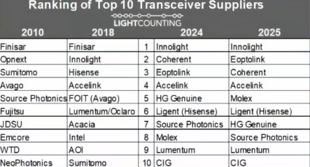
LightCounting最新发布的2025年全球光模块供应商Top10中,有7家来自中国(包括已被中资收购的Source Photonics)。
其中,中际旭创(Innolight)和新易盛(Eoptolink)据估计合计供应了约60%的NVIDIA 800G光模块需求,实际上掌控着AI数据中心最关键的“光互连管道”。
此外进入全球前十的还有:
第4名 光迅科技
第6名 海信宽带
第7名 华工科技
第10名 剑桥科技
但比较有意思的是:
中国企业虽然主导全球AI数据中心光模块制造,但是光模块内部最核心的DSP芯片和EML(电吸收调制激光器),主要还是掌握在Broadcom、Marvell、Lumentum和Coherent手中。
看起来,光模块恰恰浓缩了当今全球AI产业链的真实格局:
中国掌握规模化制造与供应链能力,
美国掌握核心器件与关键技术壁垒。
谁都离不开谁。
所以,AI时代的竞争,越来越不像单点突破,而是整条产链的较量。。。
Compute King@Compute_King
你们要的华为近封装光学模块来了。单向8T的NPO模块,用Nvidia的标准那就是双向16T,用华为的新名词就是Hi-ONE近封装光学。 一个昇腾960对应一个NPO模块。时间节点在2028年。 DSP将被绕开,之前,DSP的大部分市场份额很长时间内被博通和Marvell占据。
中文


My theory is Dario got burnt by a xmm.
Berryxia.AI@berryxia
Anthropic 的老板Dario 看来当年没少在中国花啊~ 不知道遭遇了啥如此的痛很国人……
English

@Bluebearmonkey @BetterCallMedhi @teortaxesTex @lithos_graphein @techinsightsinc @TechInsightsMFG @myteardown how did you guys not notice this in any of your teardown analysis ??
English

@BetterCallMedhi Not a chip expert here… “381 chips have already been mass-produced using these principles since 2020.”
Does that mean 381 models? Or 381 singular chips?
If it’s models, why hasn’t anyone noticed? Those tear down shops can’t tell?
@teortaxesTex @lithos_graphein
English

franchement l'annonce de Huawei hier à Shanghai vient de mettre noir sur blanc ce que j'essaie de vous faire comprendre ici depuis des années
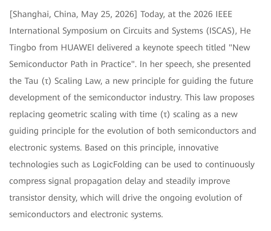
pour vulgariser Huawei vient d’annoncer au sympoisum ieee iscas une nouvelle loi physique qui remplace la loi de moore, ils l’appellent la tau scaling law et elle change littéralement le paradigme du semiconducteur mondial, en gros au lieu de continuer à rétrécir les transistors ce qui se heurte à des limites physiques quantiques infranchissables, ils optimisent dorénavant la constante de temps tau à 4 niveaux simultanément et obtiennent des gains de performance équivalents à ce que les américains atteignent avec leur lithographie euv à 200 millions de dollars la machine, sauf qu’eux n’ont pas accès à cette lithographie depuis les sanctions de 2019
la Chine dépasse donc la silicon valley sur son propre terrain et la rend périmée et ce qui se joue réellement est l'exact contraire de ce que Washington imaginait en décidant des sanctions de 2019
en ce sens je crois que très peu de gens ont pris la peine de regarder vraiment les slides de la présentation parce que le coeur de la rupture se cache ailleurs que dans le concept marketing de tau scaling law, il se trouve dans un détail technique que seuls quelques ingénieurs spécialisés ont remarqué (et que je suis parti fouiller haha), il existe visiblement un procédé de collage entre couches de silicium avec un espacement + petit que 2 micromètres, ce qui transforme les fils verticaux reliant les différentes couches d'une même puce en chemins de calcul à part entière, ils maîtrisent là l'intégration en 3 dimensions au sens fort pendant que le reste du monde raisonne encore sur un seul plan horizontal
pour moi la meilleure image c'est celle d'un architecte qui construit une tour pendant que ses concurrents continuent d'étaler des maisons individuelles à l'horizontale, intel et tsmc se battent pour graver des transistors toujours plus minuscules parce que leurs lithographies euv les enferment dans cette logique, huawei coupé de ces lithographies depuis 2019 a choisi un autre combat, raccourcir au maximum le temps qu'un signal électrique met pour traverser l'ensemble du système, cette durée qu'ils nomment tau et qu'ils minimisent simultanément au niveau du composant du circuit de la puce et de la machine complète, c'est de la physique réelle présentée dans la conférence ieee la plus sérieuse au monde sur le sujet
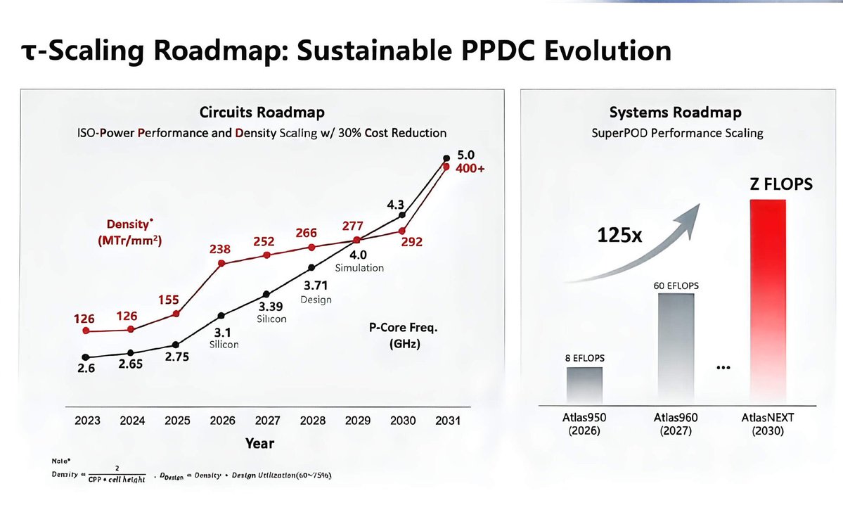
d’ailleurs les chiffres font réfléchir, allez jeter un coupé d’œil et vous allez voir que la densité de transistors monte de 126 à plus de 400 millions par millimètre carré entre 2024 et 2031, la fréquence des coeurs grimpe de 2,6 à 5 gigahertz, même la performance des systèmes complets fait x125 en 4 ans entre 2026 et 2030 & surtout 381 puces ont déjà été fabriquées en série selon ces principes depuis 2020, autant dire qu'ils ont commencé à changer de paradigme dès la première vague de sanctions américaines, 6 années de travail discret pendant que les analystes occidentaux les croyaient en mode survie mdr ce que tout le monde prenait pour de la résistance était en réalité un virage stratégique médité et mené avec la patience d'un peuple qui voit à 50 ans (la vision à très long terme de la Chine dont je vous parle souvent )
je vous le répète depuis des années ici, les sanctions occidentales accélèrent la politique industrielle et tech de Chine au lieu de la freiner, elles l'obligent à inventer le monde d'après pendant que l’occident reste coincé dans celui d'avant, d’ailleurs pour info même BYD a créé la batterie LFP face au blocage du nickel et il domine désormais le marché mondial de la voiture électrique, deepseek a conçu son architecture multi-head latent attention face au blocage des puces h100 et il a divisé par 10 le coût des grands modèles de langage, Huawei vient de poser logicfolding et tau scaling face au blocage de l'euv et il redessine déjà la trajectoire mondiale du semiconducteur jusqu'en 2031

Français


@LucaBeniniZhFe @imec_int This is what they were doing for the last 6 years and kirin chip is coming this Fall using logic folding
English

It's not easy to outperform Moore using 3D logic folding (or 3D-IC): you need to align many planets. CMOS2.0 is the program initiated by @imec_int with top research partners to address the key challenges. See CMOS2.0 position paper with solid data here: arxiv.org/abs/2510.04535
Underfox@Underfox3
Nothing that Huawei has presented was groundbreaking to those truly familiar with semiconductors; even the LogicFolding strategy is not really big news. In fact, DARPA has been testing this strategy since 2017 in the FRANC program. top500.org/news/darpa-pic…
English
@Manny1nhp @soulrambler_ It's not about gdp. It's about forex reserves. Without remittances India will be a net importer
English


India can't exist as an entity without 2 things: IT & remittances.
Internally, India is degraded & any kind of economic transition is impossible.
As the world moves on towards AI, countries like India, Pakistan, African continent will not survive the onslaught.
English
@teortaxesTex Bro can you share the paywalled article @globalsemiresearch/note/p-199162088" target="_blank" rel="nofollow noopener">substack.com/@globalsemires…
English

It'll be interesting to see how far Huawei can do with advanced chip designs despite DUV. Export control hawks conflate actual production capacity, benefits of newer process, and downstream computing power. The gap likely won't be 17x or 100x, it'll only narrow.


🌿 lithos@lithos_graphein
Jensen was right.
English
For people who didn't get what τ-Scaling is about, it actually makes a lot of sense. It's what Jensen means when he says that Nvidia's gains are OOM+ faster than Moore's Law alone would allow. it's about the raw speed of signal processing in an integrated system.
Jukan@jukan05
Huawei's latest announcement carries real significance, because China has, in effect, shown the direction in which advanced technology needs to move. And it has done so in cutting-edge semiconductors, no less. China has long been a follower. In semiconductors, Western technology played the role of the pioneer, while China was preoccupied with simply keeping pace. But by banning EUV exports to China, the U.S. manufactured a bottleneck at the lithography tool — and in doing so, it effectively forced creativity onto China. To circumvent the sanctions, China was pushed toward approaches the West had never needed to take. That is exactly what today's announcement represents. Where Nvidia co-designs memory, packaging, and logic to optimize TCO at the system level — doing it rack by rack — Huawei is doing the same thing at the chip level. I'll say it again: this is a genuinely striking approach. Memory makers are already struggling with cost scaling. As linewidths shrink, the resources required to keep shrinking them — capital, manpower, time — are climbing exponentially. So the day will come when the West, too, must make packaging, logic, and memory collaborate from the node-design stage. And it won't be far off. China, through the paradox of sanctions, has been driven to do this ahead of the West — unintentionally. This is what genuinely frightens me. As YMTC has already demonstrated, U.S. sanctions pushed China to skip the incumbent standard and jump straight to the next-generation one. The result? YMTC carved out a meaningful presence in hybrid bonding — and even Samsung, the king of NAND, ended up licensing YMTC's patents. I believe the West may well find itself licensing this Huawei technology a few years down the road. And I believe cases like these will multiply, spreading China-style standards in their wake.
English


@zephyr_z9 I got it !!!!! arxiv.org/html/2505.0557…
It's logic IP level 3d monolithic
Georgia tech paper on this was done for FPGAs
English

Looks like it's quite different from that
They are not just stacking chips on top of each other
Very clever chip design from Huawei
SkyBridge basically takes advantage of the lower resistance offered by the top metal layers
They are folding & connecting the critical data paths/wiring thru it

Alex@Alex_Intel_
@zephyr_z9 Foveros Direct 3D relabeled
English

我能想到的唯一可能是华为和 SMIC 把 ReRAM 做到金属层了,配合 EDA,搞不好真的能实现 logic 分时复用。
外汇交易员@fxtrader
华为:今年秋季面世的麒麟手机芯片性能将大幅提升。 华为公司董事、半导体业务部总裁何庭波在题为《半导体新路径探索与实践》的主旨演讲中,正式发表“韬(τ)定律”。这是中国在全球半导体领域首次提出指导产业发展的新原则。基于该定律,华为过去六年已成功设计并量产了381款芯片。今年秋季,华为将发布新的麒麟手机芯片,完整采用逻辑折叠技术,大幅提升相关性能。
中文

@isowseed_ Her name is Gigi. And I genuinely don’t gaf if you believe me or not.
English
Ain’t no fuckin way. I went on a date with this girl and she was utterly insufferable. Just kept taking pics with flash on at the dim restaurant we were in which was fine but she was also loud af. She’s also like 4 foot tall and completely flat so it felt like I was a pedo next to her. Utterly insufferable and kept comparing about finance bros while flexing her fake ass rich lifestyle. Oh and her apartment was filthy too. Girl had nothing going for her and yet claims she has “high ambitions” 💀. I blocked her immediately after the “date”.
And she’s out here complaining about the men she dates. Talk about a roach calling the kettle black
Anti-Feminism Australia@AntiFeminismAU
“When I was 20-21 in NYC I was single and ready to fuck” Now she wants to settle down.
English
Ain’t no fuckin way. I went on a date with this girl and she was utterly insufferable. Just kept taking pics with flash on at the dim restaurant we were in which was fine but she was also loud af. She’s also like 4 foot tall and completely flat so it felt like I was a pedo next to her. Utterly insufferable and kept comparing about finance bros while flexing her fake ass rich lifestyle. Oh and her apartment was filthy too. Girl had nothing going for her and yet claims she has “high ambitions” 💀
English

“When I was 20-21 in NYC I was single and ready to fuck”
Now she wants to settle down.
English
@Normal_2610 Honestly the government only cares about winning the next elections and nothing else
English

2 Wild Cards for India - In One Domain, China is not going to come & compete here. If these work out, the dividend will be huge:
> Indian Cinema
> Tourism & Culture
In both, the Govt. doesn't care. Soft Power Ignorance :)
English
@Normal_2610 Jio is all Cisco + Samsung equipment. That's no different from assembly
English
Import Import import - Assemble in India - Mental Model
CATL spent $2.58 billion on battery R&D in 2024, Reliance spent $437 million on R&D for its entire group across refining, telecom, chemicals and energy combined.
Every Indian conglomerate that promised cell manufacturing between 2021 and 2023 has settled into assembling Chinese cells into Indian containers by 2026.
They copied the Korean model of licensing foreign technology but skipped the part where Korea spent $2.1 billion a year on R&D to make the licensed chemistry their own.
India assembled the box, China kept the money.
India two biggest battery makers, Amara Raja and Exide, hold seven patents combined, CATL holds 43,000, LG holds 70,000, This is not a funding problem or a policy problem.
This is a science problem, Indian conglomerates treated batteries as a procurement exercise and are now finding out that China will not sell the answer.
Beijing October 2025 export controls shut down the licensing route entirely, You cannot buy your way to sovereignty when the seller decides to stop selling.
Reliance bought Faradion for $130 million, Lithium Werks for $61 million, took a $50 million stake in Ambri, Four years later, Faradion is still a research lab in Sheffield.
Lithium Werks makes 200 MWh a year in its Chinese plant, Ambri filed for bankruptcy after Reliance refused an $8 million bridge round, Three acquisitions, zero Indian cells.
The company that built Jio from scratch could not build a single battery cell because Jio was a bet on scale, Batteries need a bet on science, That bet has not been placed.
This is not just Reliance, Exide makes cells under a SVOLT license from China, Amara Raja runs on Gotion technology from China.
Tata Agratas runs on AESC technology owned by China's Envision, Adani's chairman visited CATL headquarters and toured their production line.
India PLI scheme promised 50 GWh of domestic cell capacity by 2025, The delivered total as of October 2025 was 1.4 GWh, all from Ola Electric, Every other major company is still importing.
Exide licensed SVOLT from China, Amara Raja licensed Gotion from China, Tata Agratas sold a 12% stake to AESC, a company owned by China Envision Group.
Cell manufacturing captures 65 to 70% of a battery value, What India calls its battery industry is mostly putting Chinese cells into Indian boxes.
Ola Electric is the only Indian company shipping vehicles with cells it made itself.
Its gigafactory runs at 2.5 GWh and is scaling to 6 GWh, with two formats now, the 4680 NMC already in thousands of scooters and a new 46100 LFP entering products next quarter.
The gap with Reliance is not money, Reliance has far more of it. Ola chose to build process knowledge inside a real factory while Reliance spent five years trying to license it from abroad.

English