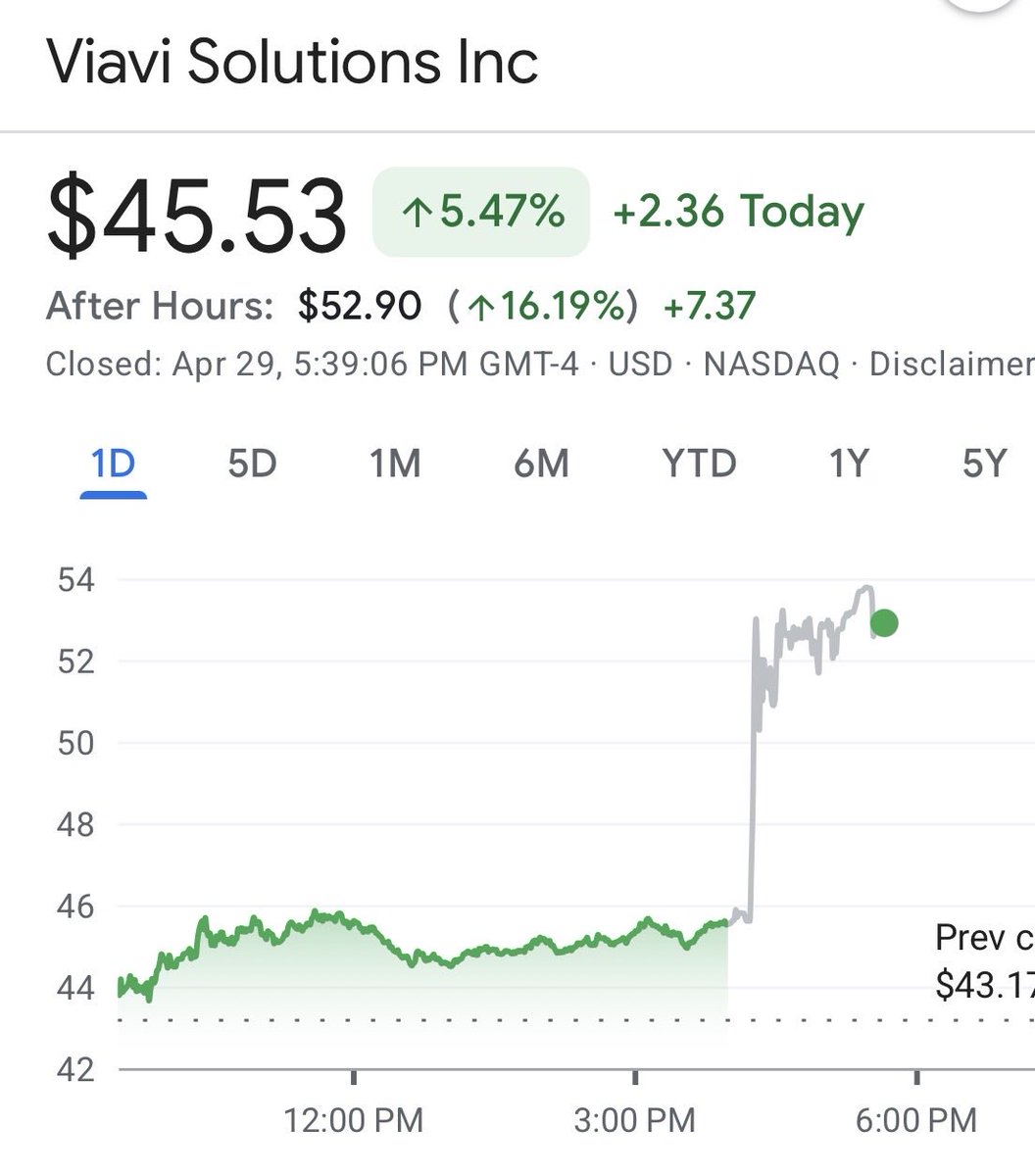
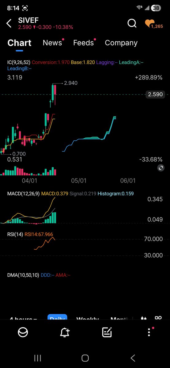
@StormDirac @michael_rigoni @PerDahlstrm @aleabitoreddit @SiversSemicond Market is deciding where price action leads. US or EU. time will tell.
English
Benjamin
5K posts

@whenthishits_
Luminary Labs. The laws of physics is the engine pushing our limits past the edge of the universe. Pierce the veil.


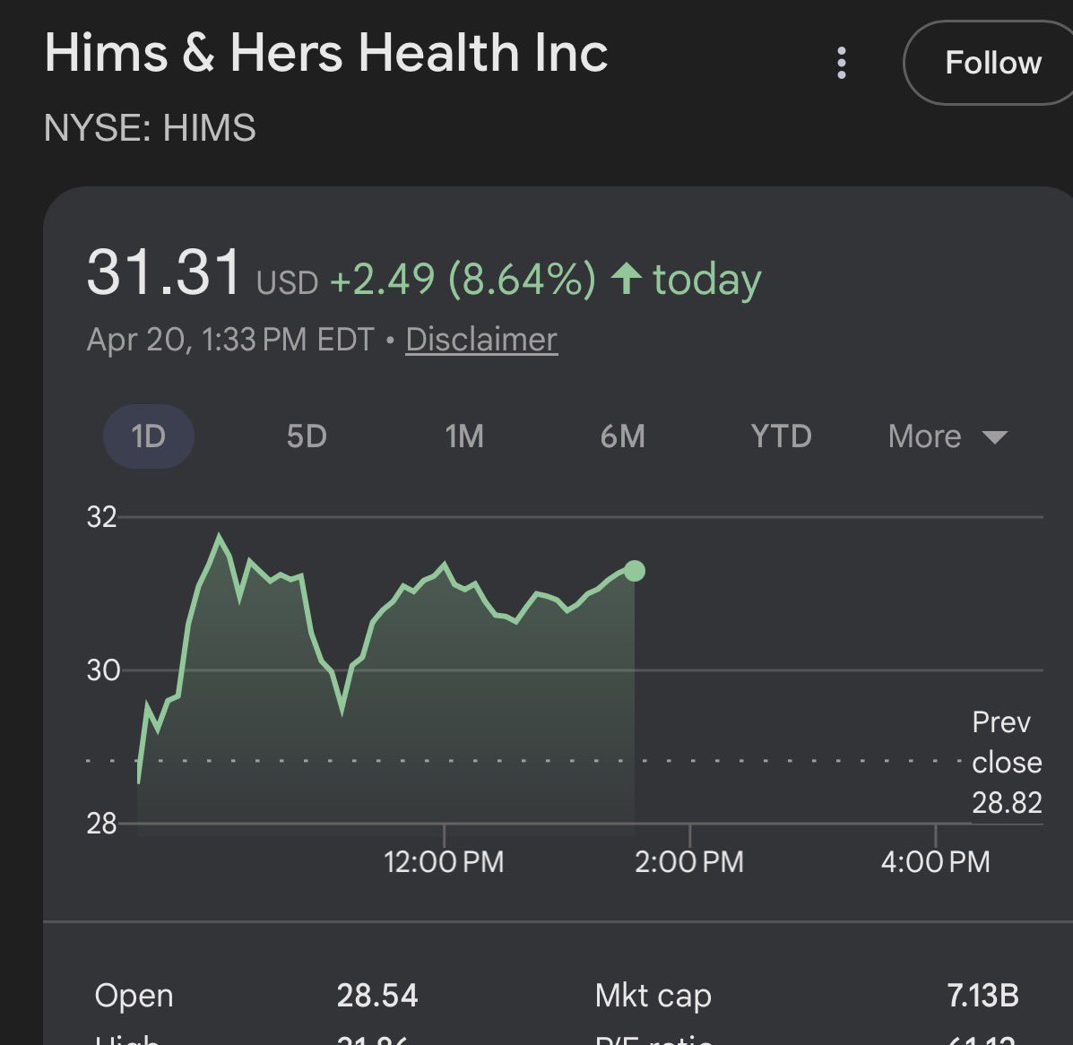
It’s still pretty incredible $HIMS is down 44% even after: 1. $NVO de-risking + partnership 2. Multiple global acquisitions expanding DTC distribution network 3. Peptide arc, with Huberman saying HIMS was set to soar under these conditions 4. Entering a friendlier macro climate. 5. Short interest reaching unsustainable 36%+ The good news is: short interest can only be so much of the float… So it’s inherent buying pressure to cover over time, which does limit downside if fundamentals improves.


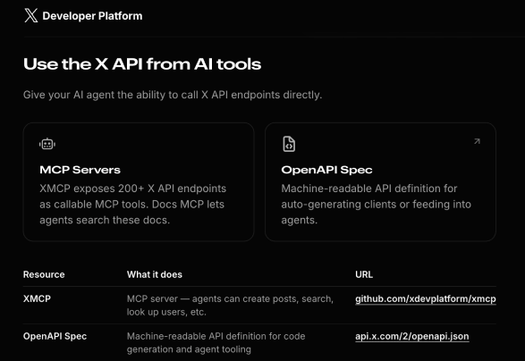
You can access 𝕏 APi via @OpenClaw. We’re trying to make it affordable without giving away the shop. Hopefully, this can be useful & fun 💫

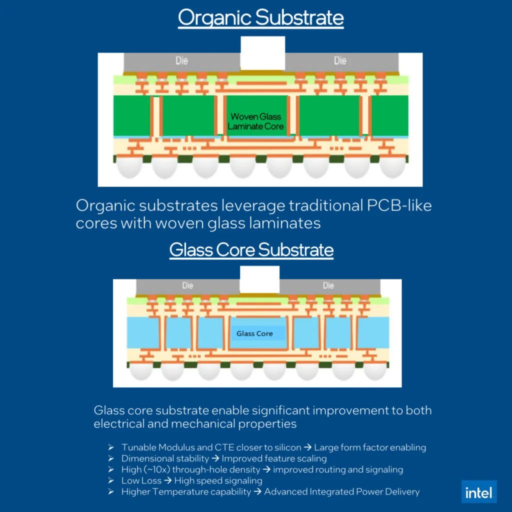

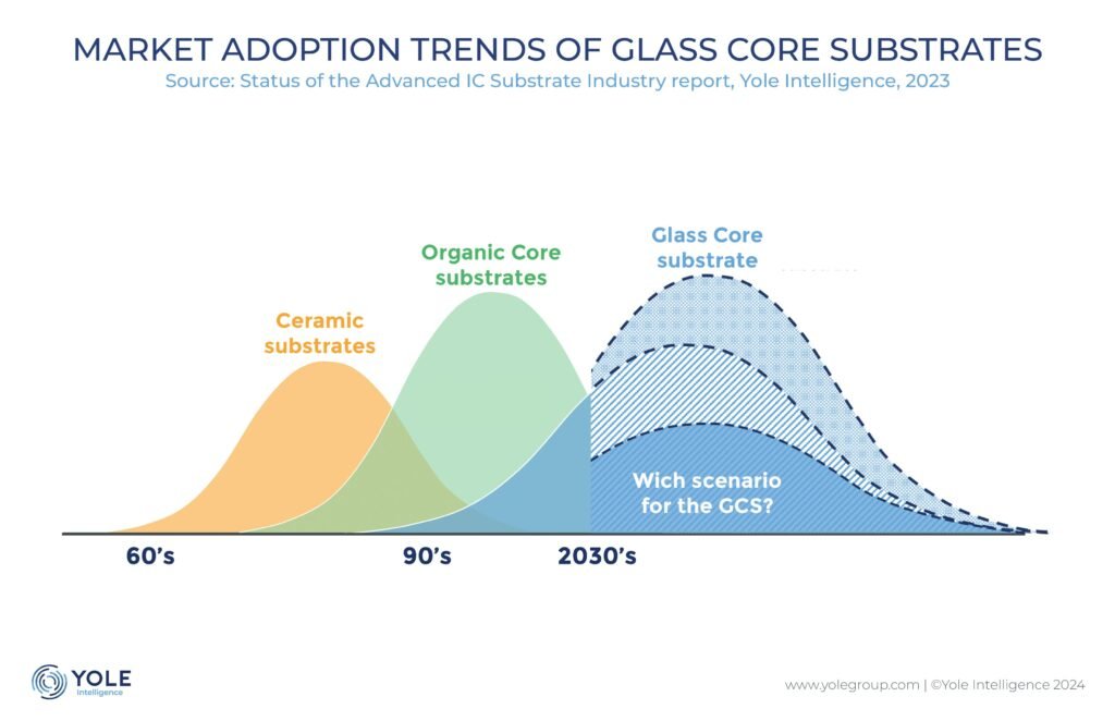
It's pretty interesting that the whole glass substrate supercycle essentially hinges on $LPK/ $LPKFF –a <€200M market cap company from Germany Glass is hitting an inflection point and the supply-chain is gearing up. Intel spent $1B+ on it. Samsung is sampling Apple. Absolics built a $600M fab in Georgia. LG Innotek is building pilot lines. Corning, AGC, SCHOTT are all supplying the glass Capex is ramping and glass looks imminent (it is) to become the base material for the next generation of leading edge semi packaging–however if you dive deeper down the rabbit hole, you’ll quickly notice that glass substrates are useless without Through-Glass-Vias, tiny microscopic holes that carry electrical signals through the glass. No TGVs, no glass substrate, no party. It's literally just a piece of overengineered glass without them That leads us to $LPK. Let me give you the surface level overview of the thesis: TGV is hard. Glass is brittle. Traditional drilling can leave micro-cracks, rough edges and stress on the glass. This can hurt reliability and lower yield which directly leads to reduced margins $LPK does things a little different. They invented a two step process which uses a laser to modify the internal structure of the glass–then a wet chemical etching process which dissolves the modified regions. No micro-cracks, defect-free holes and sub-micron precision. This process is called LIDE (Laser-Induced Deep Etching) and is currently being adopted by ~80% of the glass substrate market for their qualifications Here is the overview: - $INTC: glass substrate packaging for 18A/14A, Clearwater Forest - Samsung Electro-Mechanics: sampling Apple and Broadcom, 2027 mass production - Absolics: first CHIPS Act recipient for glass, ramping production in Georgia - $011070/LG Innotek: pilot line, partnered with UTI, targeting 2028 - $GLW: supplying substrate-grade glass compositions - AGC, SCHOTT, Nippon Electric Glass: same All of these companies are betting their next-gen packaging roadmaps on glass. $LPK holds 80% market share in qualification with a long-term goal of maintaining 70% market share once HVM starts. Based on the list above, I'll let you take a guess who will, and won't depend on $LPK moving forward