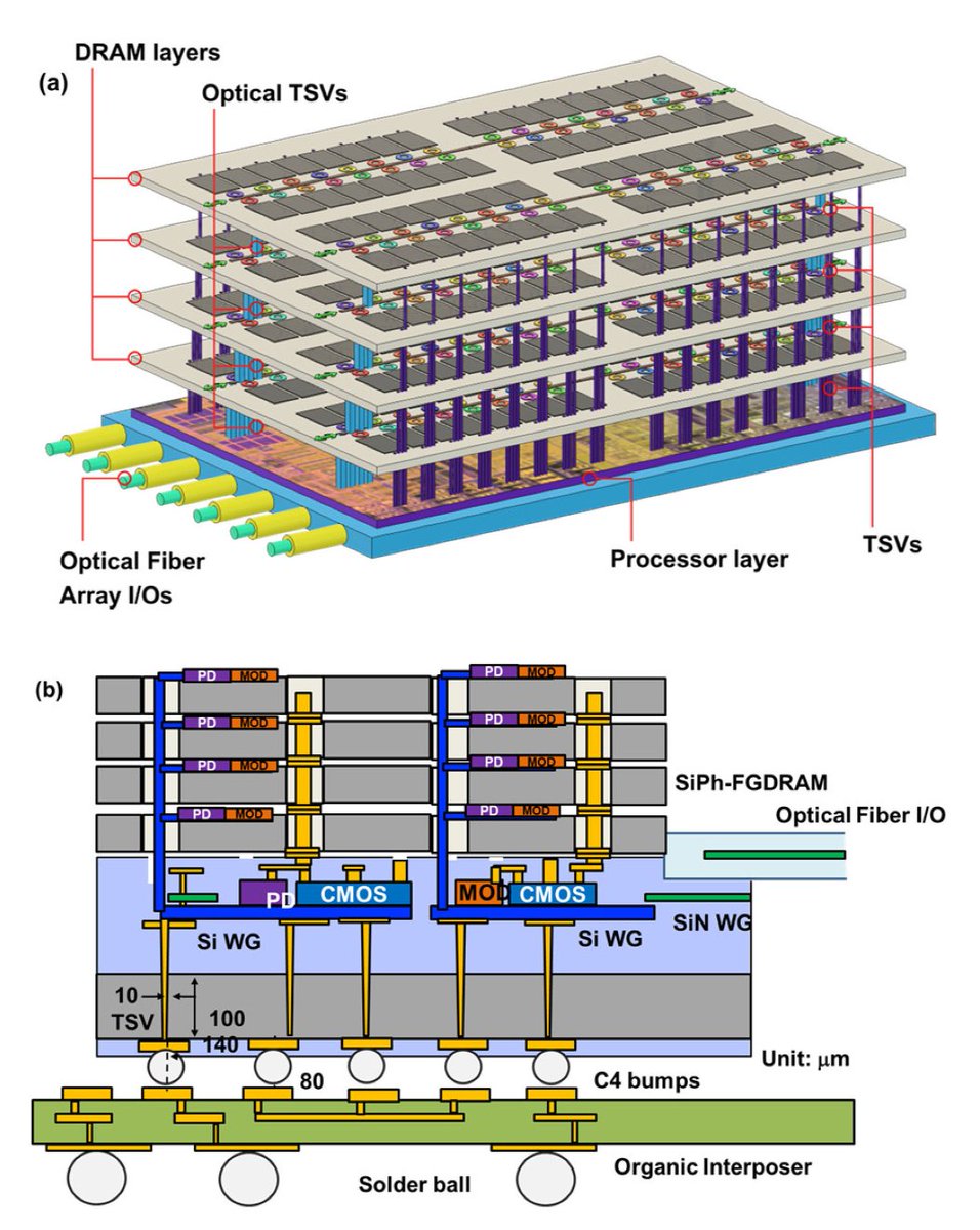
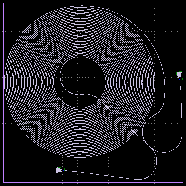
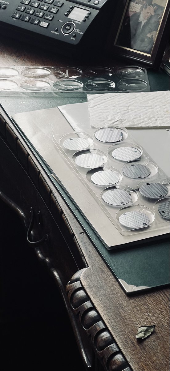
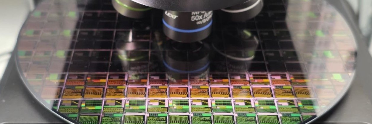
Lia

9.8K posts

Lia banner
Lia

Lia

@OptoLia

Trying to CEO @zpmtechnology, shoving silicon photonics into MEMS semiconductor sensors to accelerate autonomy in positioning & navigation

Bristol, England Katılım Şubat 2009
2.6K Takip Edilen4.4K Takipçiler
Lia retweetledi
🌿 lithos
🌿 lithos@lithos_graphein·
Terafab's decision to bring the mask shop inside the fab is not a game changer and it certainly doesn't exponentially speed up the development process. The "iterative loop" with the lithography masks that Elon was talking about last night is the design-for-manufacturing (DFM) loop. In short, this is using the mask to pattern a particular chip layer, for example, metal-1, then inspecting the outcome in various ways to identify repeating issues in the mask design. Then the software used to make the mask can be updated to fix the issue. This process loop repeats over and over again to remove yield-impacting defects from the pareto charts for each module. DFM is the most common form of fab change control because the many FMEA pieces are automated and not subjective like a physical process change would be—as in new failure modes are not up to the process engineers' imagination. With DFM, the likelihood that a mask change will create some new type of defect is very low, but this comes at the price of doing extensive verification by software means. The benefit a fab gets from bringing the mask shop in-house is minimal, only affected by the shipment of the mask itself, which is typically 1 day. This is but a small part of the DFM loop that typically takes a month or more. I put some back-of-envelope numbers for each step, and in the best case, this could be shrunk down to something like 10 days, but that would be a very rare occurrence in the chip development cycle. Keep in mind advanced lithography masks can cost $100-200k so there is also a big cost penalty to making a mask that would be DOA. My flowchart here is a very simplified depiction of this process, but it gives you an idea of how complex the loop can get for DFM.
🌿 lithos tweet media
English
20
28
205
20.8K
Lia
Lia@OptoLia·
@lithos_graphein ooowee we’d like to make some 45 deg angled slopes & this would be a nice alternative to wet etch
English
2
0
1
3.1K
Lia retweetledi
🌿 lithos
🌿 lithos@lithos_graphein·
Grayscale lithography. People crave high-tech EUV stuff, but old-school i-line litho is Space Cowboy. The MEMS world relies on grayscale lithography to print 3D patterns at the nanoscale. This is used to make microlenses, microfluidic print heads, and just about every type of sensor you can think of. The semi industry never made the ideal grayscale photoresist for the MEMS market. Instead they take typical DNQ i-line resists and, by process means, try to make them work like a decent grayscale photoresist. But this leaves so much on the table in terms of patterning performance. I dream of the ideal grayscale photoresist. Untapped market. It actually does the opposite of what a conventional photoresist does. Literally 100% opposite for contrast and etch resistance. It deserves its own special photoresist chemistry.
🌿 lithos tweet media🌿 lithos tweet media
English
1
6
53
4.6K
Lia retweetledi
Open Robotics
Open Robotics@OpenRoboticsOrg·
🏴󠁧󠁢󠁳󠁣󠁴󠁿🇬🇧ROSCon UK 2026 has been announced! 📅Dates: 21-23 October, 2026 🗺️Location: Pollock Estate Complex, Edinburgh. Additional details should be posted in the coming weeks. discourse.openrobotics.org/t/save-the-dat…
Open Robotics tweet media
English
0
4
18
983
Lia
Lia@OptoLia·
Boston! Any photonics / MEMS / inertial sensing people around 29th-3rd? We’ll be in town, keen to spend the week talking semiconductors over chowder and pie. We're bringing our own chips
English
0
0
2
114
Lia
Lia@OptoLia·
@jwt0625 i’m shocked how much it’s bending upwards - it’s like beyond “MEMS” levels of size scale usually i’d hate an out of plane bend mode like this but if it’s in a vacuum and not on a moving platform its pretty cool
GIF
English
0
0
2
104
Lia retweetledi
National Gallery of Art
I am Harry, a Harvard educated curator ready to slay the house down boots. Today is the day I yoink control from the social girlies and Ali the mother of all rizzlers. They will not stop my aura. Siri add painting emoji here thanks
English
122
1K
7K
847.2K
Lia retweetledi
The Nobel Prize
The Nobel Prize@NobelPrize·
Today we celebrate Leo Esaki, on his 101th birthday. He was born on this day in 1925 in Osaka, Japan. While working in the Sony Corporation research laboratory in Japan, Esaki used some deceptively simple experiments to prove the existence of a new kind of tunneling phenomenon in a semiconductor. His discovery also showed that this effect could be used technically in so-called tunnel diodes. Esaki’s discovery opened up a new field of research and initiated intensive and successful developments at many international research laboratories. Esaki was awarded the 1973 Nobel Prize in Physics jointly with Ivar Giaever for their experimental discoveries regarding tunneling phenomena in semiconductors and superconductors, respectively. Watch our 2004 interview: bit.ly/41msN6G
The Nobel Prize tweet media
English
22
216
994
58.5K
Lia
Lia@OptoLia·
@mov_axbx @yacineMTB what part of the xmos chip would sense the inertial forces?
English
0
0
0
72
Nathan Odle
Nathan Odle@mov_axbx·
I was going to build an IMU out of an old xmos chip 10 years ago You could do imu / esc / main computer with these chips no rtos required and everything deterministic even across the links Idk why more people don’t use them but their predecessor transputers were in defense satellites
English
2
0
5
2.7K
kache
kache@yacineMTB·
what kind of microcontroller should i run for my tiny ESC? I'm thinking an STMG
English
23
0
33
7.1K
Lia
Lia@OptoLia·
@PhotonCap @samsoniuk i’ve not seen a universally used PIC-type isolator yet - it would be a huge win for a foundry to produce a PDK one! No issue with a bulk isolator but imo it’s such a key component to miniturise on chip overall - irrespective of this work
English
1
0
2
30
Photon Capital
Photon Capital@PhotonCap·
@OptoLia @samsoniuk isolator can prevent reflection? the light is guided by 3D waveguide. Ben Yoo's team is good at 3D waveguide fabrication (it is indeed amazing) but I have also still the same veiw on back reflections where the waveguide is bent.
English
1
0
1
64
Photon Capital
Photon Capital@PhotonCap·
Concept image for architectures showing optical vias and optically connected memory (a) 3D stacking of silicon-photonic fine-grain electronic DRAM dies with the silicon photonic logic layer at bottom vertically interconnected by through-silicon-optical-vias (TSOVs). (b) Proposed SiPh-FGDRAM utilizing silicon-photonic CMOS DRAM mini-bank dies in multi-stacks including the silicon photonic logic layer at the bottom. "Scalable 3D Silicon Photonic Electronic Integrated Circuits and Their Applications," in IEEE Journal of Selected Topics in Quantum Electronics, vol. 26, no. 2, pp. 1-10, March-April 2020, Art no. 8201510, doi: 10.1109/JSTQE.2020.2975656
Photon Capital tweet media
Photon Capital@PhotonCap

3D optical memory concpet image details will be provided soon

English
7
60
409
26.6K
Lia
Lia@OptoLia·
@macjshiggins almost came up with a witty version of “touch grass” but like “touch ground truth” whilst reading the thread what measurements…!
English
0
0
1
148
MacCallister Higgins
MacCallister Higgins@macjshiggins·
exquisite slop. labeled ’26, but unmistakably ’24 on the palate. few generated responses miss the point with this level of conviction. a 3o masterpiece.
Nengjia Li@nengjiali

@hissizheyvan you're completely right about the double integration drift. And it's why ESKF is so powerful. it uses the IMU for high freq motion while constantly using external measurements to zero out that drift in real-time

English
7
0
105
7.1K
Lia
Lia@OptoLia·
@usgraphics some of us trying to recreate the vibe of msn messenger i’ll be the one to say it - we use Teams because it’s plain & dosnt have that Slack, slackness?
English
0
0
1
117
U.S. Graphics Company
U.S. Graphics Company@usgraphics·
Maybe we should just use IRC for internal comms. I remember working at a 150 people “startup” and it was embarrassing how everyone is memeing and constantly glued to Slack. The whole experience left a bad taste about modern HR centric workplaces. Email + IRC + Telephone would be based. No emojis, no memes, no files, no photos. Asyn/sync be damned. Phone rings, I’m answering “Department of Flutter Dynamics, how may I help you?”
U.S. Graphics Company tweet media
English
48
28
830
51.4K
Lia
Lia@OptoLia·
@qdaicho its a small world! in germany? wow do you remember what event? may the lithography gods be with your wafer - it’s a really nice dense design so fingers crossed
English
1
0
1
65
Daian Chow 🍁
Daian Chow 🍁@qdaicho·
@OptoLia I believe I may have met you in Germany! And yes that was an important design consideration. I will find out how effective my design is once it passes characterization.
English
1
0
0
55
Lia retweetledi
Steven Pang
Steven Pang@thewildstevenp·
A 10-minute application for $100,000. A free, no-strings-attached prize for builders, scientists, operators. Introducing the Eigenprize. ↓ run by @menemazarakis, @markkhrapko, & yours truly :)
Steven Pang tweet media
English
80
150
827
1.3M
Lia
Lia@OptoLia·
looks like I’ll have to eat our chip
Lia tweet media
English
0
0
5
131
Lia
Lia@OptoLia·
@sokol_cc either ends up being fancy coasters or a game changer! how we feel when our wafers come home
English
0
0
1
378
Sokol
Sokol@sokol_cc·
I just secure 160 wafers with very specific chip from 1978. They are on plane right now. Those chips are priceless for me and have big commercial value. I got them free of charge after very quick gentleman’s agreement. I love to move in high trust society.
Sokol tweet media
English
28
9
527
167.5K