Sabitlenmiş Tweet

Isabel
715 posts
@beamshift
making things happen with electron microscopes🔬 she/her 🐘: https://t.co/R0PzrAHGxy 🦋: https://t.co/q3MDRCDoc5
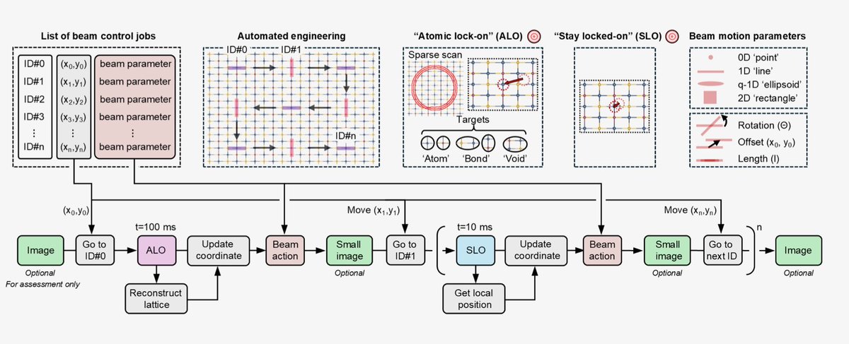
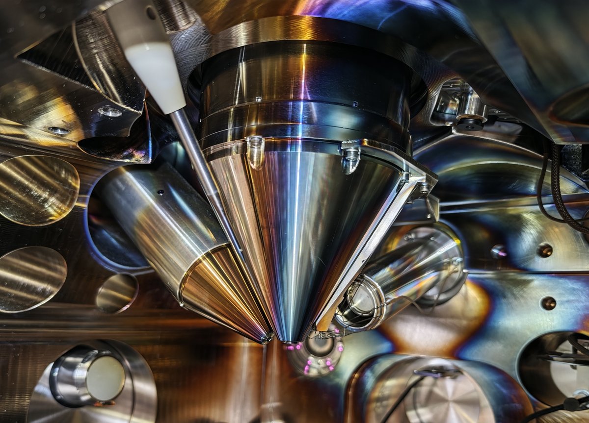
closed loop & vectorized scan control enables some really interesting stuff!


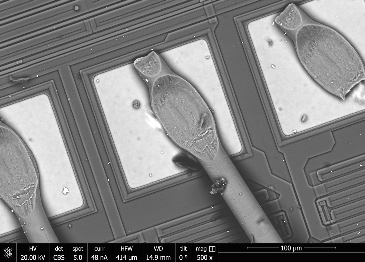
you don’t need to do this unless your son is an electron microscope
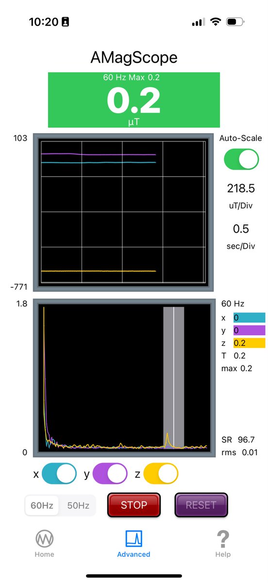
For everyone who asked- This was my temporary “emergency made” faraday that I made around my son’s bed until we moved. It significantly reduced the radiation from the nnEMF from the 5G tower (~80microwatts) keeping him protected while he slept was (at a minimum) my priority.
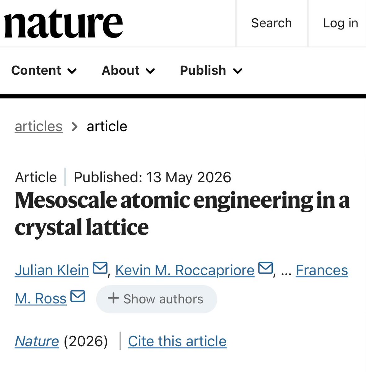
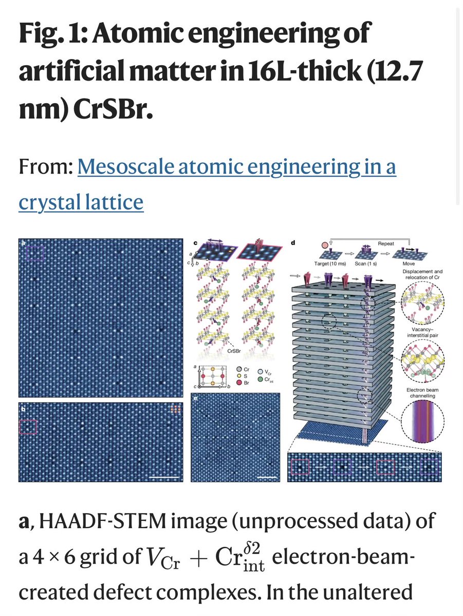
Autonomous atomic-scale fabrication: ML-guided electron beams sculpting 2D materials Functional properties of 2D materials like MoS2 are exquisitely sensitive to atomic structure. A metallic Mo6S6 nanowire along a hole edge in semiconducting MoS2 yields a 1D-2D heterostructure with electronic behavior nothing like the pristine monolayer. Building this atom by atom means ejecting sulfur atoms at chosen sites, and earlier automated workflows leaned on lucky statistics, with success rates near 64%. Zijie Wu and coauthors build a fully autonomous platform that closes the loop between imaging, ML, and beam control in a STEM. After each HAADF acquisition, three lightweight models decode the image: a U-net ensemble (ELIT) locates atoms, a second U-net segments collapsed MoS-nanowire regions, and a random forest classifies each site as Mo, S, or sulfur-vacancy-line. The classifier learns from 55 hand-labeled neighborhoods, each encoded by distances and intensity to the 5 nearest atoms. No huge simulated datasets, no GAN style transfer, no foundation model. Selected sulfur sites go to an FPGA-controlled scan routine that places the beam in Archimedean spirals with radially symmetric dose. Three strategies are shown: targeted nanowire growth along a pore edge, freestanding MoS-NWs between two seed pores, and directional growth using DBSCAN and line fitting on the largest cluster. The directional case reaches 65% success over 42 runs, with decoding in about 1 second on a GPU. What stands out from an ML-for-science angle is the deliberate small-data philosophy. For atomic labeling, big vision models trained on simulated images often transfer poorly to experiments. Pairing simple models with intuition-based feature engineering is faster to deploy and easier to tune. For applied R&D in semiconductors, quantum devices, and 2D electronics, this reframes what atomic-scale design means. Teams can specify a target defect topology and let the platform iterate toward it without massive labeled datasets, and the framework should transfer to other TMDs, making it relevant for catalysis, energy materials, and quantum sensors. Paper: Wu et al., npj Computational Materials (2026) — CC BY 4.0 | doi.org/10.1038/s41524…