
Mr. Vinyl 美股投资之路
158 posts

Mr. Vinyl 美股投资之路
@JayLiu2908
追求超高回报,坚持价值投资、长期主义。 Seeking high returns, stick to value investing and long-term principles.
Kenya Katılım Ocak 2026
193 Takip Edilen22 Takipçiler


@RT_com They don’t have to accept them. No one asked. Sanctions will still be implemented.
English


Mr. Vinyl 美股投资之路 retweetledi

Mr. Vinyl 美股投资之路 retweetledi

Mr. Vinyl 美股投资之路 retweetledi
Mr. Vinyl 美股投资之路 retweetledi

$GOOGL TPU infrastructure supply chain
Optical Modules & High-Speed Interconnect Chips
$COHR, $AAOI, $LITE, $MRVL, $CRDO, $SMTC, $MTSI, $FN
OCS (Optical Circuit Switch)
Coherent, Lumentum, Fabrinet
Server Power Supplies
$MPWR, $AEIS, $VICR
PCB - $TTMI
ASIC Design & IP - $AVGO
Wafer Manufacturing & Advanced Packaging
$TSM, $AMKR
System Assembly & EMS Manufacturing
$CLS, $JBL, $FLEX
Semiconductor Wafer Test & Probing
$FORM
Memory (HBM / NAND exposure)
$EWY, $MU, $SNDK
Liquid Cooling / Thermal Management
$VRT, $MOD, $NVT
CPU - $ARM
MPO and AOC (High-Density Interconnect Cables)
$APH, $TEL, $GLW

English
Mr. Vinyl 美股投资之路 retweetledi

$AMKR 是一家美国本土外包半导体封测服务商,自1968年创立以来一直是半导体封装外包服务的开创者,是苹果、英伟达等全球顶级芯片公司和电子OEM的战略制造合作伙伴。
最近发布的2026Q1财报营收$1.685亿,同比+27%,创Q1历史新高;毛利润$2.39亿,毛利率14.2%超指引上限(指引区间12.5%-13.5%);营业利润$1亿,营业利润率6%,同比大幅改善360基点;EBITDA $2.85亿,EBITDA率16.9%。
这次的增长贡献来自几个维度:
1️⃣通讯(智能手机/平板)同比+42%,是本季增长最强的板块,高端旗舰机型需求驱动;
2️⃣计算(数据中心/AI/PC)同比+19%,AI数据中心营收创历史新高;
3️⃣汽车与工业同比+28%,先进封装营收亦创历史新高。
先进封装已经越来越成为关注重点。这也正是 $AMKR 在讲的故事。同时AI成为新的增长引擎。Amkor CEO在财报电话会上确认,AI先进封装业务预计今年将同比翻三倍(3x);目前已有超过5个客户正在进行HDFO和硅中介层技术的资格认证,处于不同认证阶段。
摩根大通的TSMC后端报告明确将Amkor列为TSMC越来越依赖外部合作伙伴承接CoWoS-S封装项目的主要受益者,投资逻辑从"亚洲消费类OSAT"向"全球AI先进封装平台"根本性转变,战略杠杆涵盖台积电、英伟达、苹果和博通。
去年10月开始动工的亚利桑那工厂也是该公司的战略布局。那是一座先进封装和测试工厂,总投资$20亿,获得美国商务部CHIPS法案最高$4.07亿直接资金补贴,另有$2亿贷款授权;该工厂紧邻台积电亚利桑那晶圆厂,预计2028年开始运营,主要客户包括苹果和英伟达。
这背后的逻辑:美国政府希望把整个芯片供应链——从晶圆制造到封测——都迁回美国本土,Amkor是这个战略的核心执行方之一
Fiona ❤️& ✌️@nft_hu
整了了一下目前公布的财报Beat的 #半导体 #光通讯 #AI基建 公司的情况: highlight一些大超预期的公司: $ASML 光刻机:超预期 / 上调全年指引上调至€360-400B;记录积压订单€38.8B;EUV垄断地位稳固 $AMKR 先进封装需求全面爆发,强劲创营收历史记录;AI端市场需求旺盛 $CIEN 双线超预期 / 大幅上调积压订单$70亿;全球最快1.6T;摩根士丹利目标价$380-400;AI数据中心互联需求爆发 $FN 大幅超预期,营收$1.13B,YOY+36%,光通信营收+36%;HPC业务环比+473%;深度绑定Lumentum等光通信巨头 $AAOI 超预期,营收$150-165M,全年指引上调,800G/1.6T月产能目标+400%至50万只;2026年营收目标>$10亿;美国本土制造商战略优势。 $ANET 营收强劲,YOY+33-34%,全年指引上调至+40%;Needham预计Q1营收增速超33-34%;AI后端网络核心受益者 $NOW 全面超过,营收$3.77B,YoY+22%,上调全年订阅收入;Now Assist百万级客户YoY+130%;CRPO+22.5%。 $GEV 大幅超过,不过有特殊结算原因。YoY794%;积压订单$163B ;Q1数据中心电气化订单$2.4B超全年2025;FCF $4.8B翻四倍;股价当日+14%。 完整表单见图片
中文
Mr. Vinyl 美股投资之路 retweetledi

他说的很好,我想重点说一下 “Why now”的问题。为什么是现在,为什么之前没有这个需求。
$AEHR 做的事情叫晶圆级老炼(Wafer-Level Burn-In, WLBI)和封装级老炼(Package-Level Burn-In, PLBI)。
老炼是什么?简单说:在芯片出厂前,给它施加高温+高电压+工作负载,持续数小时到数十小时,让那些有隐性缺陷的芯片在工厂里提前死掉(“早夭筛选”),而不是到了客户手里才死。
为什么这个概念,现在开始炒而不是一年前开始炒?两个方向,分别是自研高功耗ASIC芯片和硅光。
1. 自研ASIC芯片这一点是最近开始多起来的,每种定制ASIC都是全新设计的芯片,在量产初期良率不稳定,这时候老炼的价值最大。而NVIDIA的GPU已经是成熟产品,老炼流程是标准化的。新ASIC的老炼流程需要从头定制, $AEHR 正是做这件事的公司。
那么大家可能要问了,那之前 $goog 家tpu的老炼是谁做的?这一点,查不到。Claude老师认为,因为之前TPU的功耗只有200-300W,一些粗糙的方法就足够了,功率没有那么夸张的时候,老炼不是一个必不可少的流程,这是一个因为AI ASIC功耗爆炸而新出现的需求空白。
那么又有朋友问了,这公司之前主要是做sic车机芯片的老炼,难道车机芯片功耗比TPU还高?不是的,车机芯片是因为SiC的晶体工艺本身麻烦,并且车机对于安全的需求是苛刻的。
2. 硅光,
第一步:硅光芯片以前需要老炼吗?
硅光芯片不是新东西,2015年前后就开始商业出货了。但那时候硅光芯片被封装在pluggable光模块里。一个OSFP光模块坏了怎么办?拔掉,换一个新的,30秒搞定。光模块的单价几百到几千美元。
在这个架构下,硅光芯片的老炼需求很弱。为什么?因为现场故障的代价很低,换一个光模块的成本远低于对每颗硅光芯片做全检老炼的成本。经济学上不划算。大多数光模块厂商做的是常温功能测试+高温老化抽样,不是每颗芯片的晶圆级全检老炼。
第二步:什么变了?
两件事同时在变:
变化一:产量从百万级走向千万级甚至更多。
之前数据中心的光模块用量是百万级/年。现在AI集群的规模在爆炸,一个10万GPU的训练集群可能需要几十万个光模块。全球hyperscaler同时在建多个这样的集群。硅光芯片的年产量正在从百万级跳到千万级。
产量一旦到了这个规模,即使只有千分之一的早期故障率,每年也意味着几万颗芯片在客户现场死掉。每一颗死掉的芯片都意味着一个光通道中断→可能影响GPU之间的通信→可能导致训练任务中断或性能降级。在一个几千万美元的训练任务中,光模块故障导致的停机成本远远超过光模块本身的价格。
所以第一个驱动力是:产量跨过临界点后,“可接受的故障率”的经济学计算完全改变了。
变化二:CPO/NPO让硅光芯片变得不可更换。
这才是最关键的变化,直接连接到我们之前讨论的CPO架构。
在pluggable时代,光模块是可热插拔的。硅光芯片坏了=换一个光模块=$几千美元。
在CPO时代,硅光引擎被直接封装在交换芯片或GPU的package里面。硅光芯片坏了=整个package报废,包括那颗价值几千到上万美元的交换芯片/GPU,包括昂贵的HBM堆叠,包括复杂的先进封装结构。一颗几百美元的硅光芯片的故障,代价瞬间从”换一个光模块”变成了”扔掉一整个价值几万美元的封装”。
这就是“不可更换性驱动”的本质:当一个零件从”可插拔”变成”焊死在里面”的那一刻,它的可靠性要求跳升了一个数量级。
这跟SiC的逻辑有相似之处,SiC的老炼需求也不是因为SiC本身有多贵,而是因为SiC失效后的连带后果不可接受(人命)。硅光在CPO中的老炼需求也不是因为硅光芯片有多贵,而是因为失效后的连带成本不可接受(整个封装报废)。
第三步:为什么需要晶圆级老炼?
硅光芯片有一些特殊的失效模式是常温功能测试发现不了的:
波导缺陷:硅波导中的微小缺陷(刻蚀粗糙度、材料杂质)在常温下可能不影响光传输,但在高温长时间工作后会导致插入损耗逐渐增大,最终超过系统容限。
调制器退化:硅MZM中的掺杂区域在高温高压下可能发生离子迁移,改变调制器的Vπ(半波电压),导致消光比下降。
锗探测器暗电流漂移:Ge PD的暗电流对温度和时间敏感——有些探测器在几百小时的工作后暗电流会显著增大,恶化信噪比。
光栅耦合器/边缘耦合器对准漂移:封装后的热循环可能导致耦合效率逐渐下降。
这些问题的共性是:常温短时间测试看不出来,但在实际工作条件下几百到几千小时后会暴露。 老炼的作用就是用加速应力在几十小时内把这些”慢性病”提前诱发出来。
而且因为硅光芯片是在晶圆上制造的(SOI晶圆,Soitec供应,TSEM代工),在晶圆阶段做老炼(WLBI)比切割封装后再测效率高得多——一片300mm晶圆上可能有几百颗硅光die,AEHR的FOX-XP可以一次性对整片晶圆做全检。
AEHR为其主要硅光客户升级了FOX-XP至新的高功率配置,在九片晶圆配置中每片晶圆可达3.5kW功率,并配备了全自动化的WaferPak Aligner,可以一次性对300mm晶圆上所有器件进行测试和老炼。
Paradis Labs@ParadisLabs
The most asymmetric AI supply chain setup atm is $AEHR. A $1B company with a literal monopoly. Seen it gain some traction on X these past few weeks/months, but not really seen a proper deep-dive. They make burn-in test systems — equipment that stress-tests chips at full operating power before they ship. Every GPU, every custom ASIC, every AI accelerator inside a hyperscaler data center has to be tested. You cannot ship a $10K chip that fails after 200 hrs. $AEHR tests entire 300mm wafers simultaneously — at up to 3,500 watts per wafer, thousands of amps of current. No other company on earth does this. $TER and Advantest are the giants of chip testing. They test chips individually or in small batches. $AEHR tests entire wafers before packaging. It's a completely different point in the manufacturing process — and it means defects caught before expensive packaging. They also just became the first company to ship wafer-level burn-in systems for AI processors. That's an actual $14M order delivered in Feb'26. The two platforms driving the AI thesis FOX-XP (Wafer-Level Burn-In) → Up to 9 × 300mm wafers in parallel → 3,500W per wafer — unmatched → $14M order received Feb 26 for AI processors → Silicon photonics follow-on order early March → Used for: AI processors, SiC power, optical chips Sonoma (Package-Level Burn-In) → Acquired via Incal Technology → Up to 2,000W per device — for packaged AI ASICs → First hyperscaler production win: Feb 11, 2026 → 10 companies visited HQ to evaluate → "Very large expansion" of orders guided for H2 2026 Three orders in 30 days. Two platforms. Both now confirmed in AI production. But the consumables angle is what most people miss Every system $AEHR sells locks in a recurring revenue stream. WaferPak contactors, DiePak carriers, and BIM consumables are proprietary, device-specific, and must be replaced regularly. This is razors-and-blades applied to semiconductor test equipment. Each FOX-XP system sold = years of consumable revenue at high margins. The installed base compounds. FY22–FY24: SiC/EV drove explosive growth. Revenue went from $22M → $65M. Gross margins hit 50%. Operating margins 20%+. FY25: EV programs delayed across the board. OEMs pulled back on SiC orders. Revenue fell to ~$60M then kept falling. Q2 FY26: $9.9M revenue. Gross margin: 29.8%. The stock got obliterated. Down 80%+ from peak. And then the AI orders started coming in. Q2 FY26 revenue: $9.9M ← confirmed trough H1 FY26 revenue: $20.9M (−21% YoY) H2 FY26 guidance: $25–30M revenue H2 FY26 bookings guidance: $60–80M That bookings number is the key figure. Management was explicit: the $60–80M is based on specific customer forecasts provided to $AEHR — not internal projections, not aspirational targets. Customers told them what they plan to order. Bookings in H2 FY26 ship and recognize as revenue in FY27 (which starts June 2026). FY27 is the inflection year. Management has stated the AI processor TAM is 3–5× larger than the SiC/EV market that drove the FY22–24 peak. Think about what that means: - Peak SiC revenue: ~$65M - If AI TAM is 3–5×: $195–325M revenue potential - Current market cap: ~$400M You're paying ~1.2–2× peak revenue for a company at trough, with a confirmed monopoly position, zero debt, and three orders in the last 30 days. The balance sheet is a genuine differentiator Zero long-term debt. ~$31M cash. No equity raises since the downturn. Compare that to $ENTG with $3.4B net debt from the CMC acquisition, or $LWLG burning $21M/year pre-revenue. $AEHR can execute without diluting you. But it's not a layup 1. Extreme lumpiness. Systems are $3–5M+ each. One delayed order swings quarterly revenue 30%+. This has happened multiple times. 2. Customer concentration. A handful of hyperscalers likely represent 80%+ of near-term bookings. Any program cancellation is devastating. 3. Gross margins still compressed. 29.8% last quarter vs. 50% at peak. Recovery requires volume ramp to arrive on schedule. 4. SiC is still dead weight. Legacy EV exposure hasn't recovered and occupies capacity. TLDR: $AEHR has a monopoly on a process that is physically required to ship AI processors at scale. Revenue is at a confirmed trough. Three orders have arrived in 30 days. Management has reinstated specific bookings guidance ($60–80M H2) based on customer forecasts. FY27 is the inflection. The balance sheet is clean. The TAM is 3–5× the peak that drove the last cycle.
中文
Mr. Vinyl 美股投资之路 retweetledi

Mr. Vinyl 美股投资之路 retweetledi

$SNDK 这份财报,单看数字几乎是炸裂级别,但股价盘后一度跌超 8%。
我看 Serenity @aleabitoreddit 的观点,说得挺到位。存储股的财报可预测性其实比较强。她之前就根据第三方 NAND / DRAM 涨价数据,推过 $MU 的毛利率,最后和财报公布结果差不多。
$MU 财报后也是大跌,因为价格调整往往发生在财报前,而不是财报当天。
NAND / DRAM 涨价、毛利率弹性、供需缺口,这些专业投资者在财报前就能大致算出来。
所以 $SNDK 这次主要还是 4 月已经涨得太多了。
存储涨价、AI 服务器需求、NAND 反转,这些逻辑已经提前被市场打进股价里。到了财报公布的时候,市场就会更关注有没有比大家提前算出来的更好。
管理层这句话我觉得很关键:
“本季度标志着 SanDisk 的一个根本性转折点——我们的技术领导力正在推动我们有意转向最高价值的终端市场组合,由数据中心引领。”
由此看闪迪不只是吃一轮 NAND 涨价周期,而是在往更高价值的 AI / 数据中心需求迁移。
所以我个人看法是短期回撤,更像是预期太满后的降温。
但中期逻辑,并没有因为盘后一跌就被证伪。
如果产业逻辑没坏,回撤反而是重新评估加仓点的机会。

中文
Mr. Vinyl 美股投资之路 retweetledi

市场参与者对$AXTI存在致命误解,总把这家公司的价值单纯绑定在住友的磷化铟衬底业务上,这是完全错误的判断,也是做空者踩坑的核心原因!
首先必须明确:$AXTI在整个磷化铟供应链中,占据的份额远超40%,这也是专业机构重金布局它的核心逻辑。这家公司真正的实力,是掌控了磷化铟产业链上多个关键瓶颈环节,绝非单一的磷化铟衬底业务。
供应链就像精密运转的体系,哪怕只切断20%的供给,都会引发灾难性的连锁反应,而$AXTI把控的远不止一个环节,而是3-4个核心瓶颈节点,一旦发力,下游产业将直接陷入停摆。
一、核心原材料端:形成绝对双寡头垄断
铟、镓、锗这些磷化铟必备原材料,AXTI(自有产能+金美产能)联合Vital,与国内相关企业形成原材料双寡头格局。西方企业比如5N等,在这个领域市场份额微乎其微,全球绝大多数原材料供给,牢牢掌握在Vital和AXTI手中。
二、pBN坩埚:另一大核心供应链瓶颈
pBN坩埚是磷化铟生产的关键耗材,$AXTI通过博宇布局,再次掌控这个核心瓶颈。全球范围内,除了信越、摩根等少数玩家,几乎没有其他竞争者,这是磷化铟精炼环节的又一供给命脉。
三、磷化铟衬底:双寡头主导,其他玩家毫无竞争力
在磷化铟衬底环节,AXTI与住友形成绝对双寡头,JX、COHR等企业的市场份额可以忽略不计。
整个磷化铟生产链条,还涉及红磷、日本化学/拉莎等中间环节,而AXTI把控的上游材料和精炼产能,是所有下游厂商绕不开的壁垒。**COHR根本无法独立生产磷化铟衬底**,脱离$AXTI掌控的上游原材料与精炼产能,完全无法实现量产。
一直以来,LITE的CEO都在为磷化铟衬底供给问题彻夜难眠,西方超大规模数据中心的持续建设,离不开磷化铟的稳定供给,50亿美元的相关估值在供应链断供风险面前,毫无意义。
当下日本还在持续加码上游材料出口管制,而$AXTI几乎把磷化铟全产业链的上游关键资源全部攥在手中。
$AXTI的价值从来不是“磷化铟衬底制造商”,而是覆盖铟镓锗原材料+精炼加工+pBN坩埚+磷化铟衬底的全产业链把控者,最终和住友共享磷化铟衬底双寡头地位。
一旦Vital联合AXTI切断上游多个瓶颈环节的供货,西方所有磷化铟衬底下游企业都会被波及,AXTI本质就是磷化铟领域的小型垄断者。它的估值逻辑,源于对整个供应链的绝对掌控,可惜很多机构分析师都没看透这一点,盲目做空$AXTI,注定要付出代价!
中文
Mr. Vinyl 美股投资之路 retweetledi

Google didn’t just launch new TPUs. They split the AI stack.
Training vs inference, separate lanes now. That’s a big deal.
More compute → more interconnect → more power → more cooling.
Follow the chain:
$MRVL $CRDO (data flow)
$COHR $LITE (optics)
$MPWR $VICR (power)
$VRT (cooling)
$TSM $AMKR (build it)
This isn’t one trade. It’s an ecosystem shift.

English
Mr. Vinyl 美股投资之路 retweetledi
Mr. Vinyl 美股投资之路 retweetledi

Mr. Vinyl 美股投资之路 retweetledi

Mr. Vinyl 美股投资之路 retweetledi

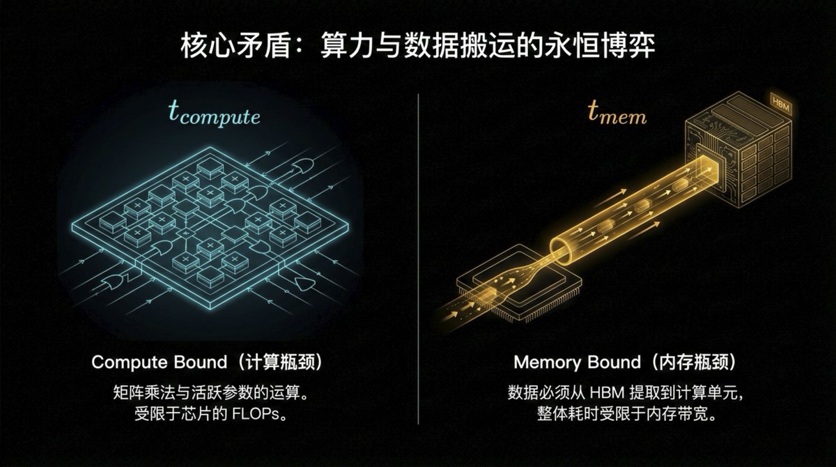
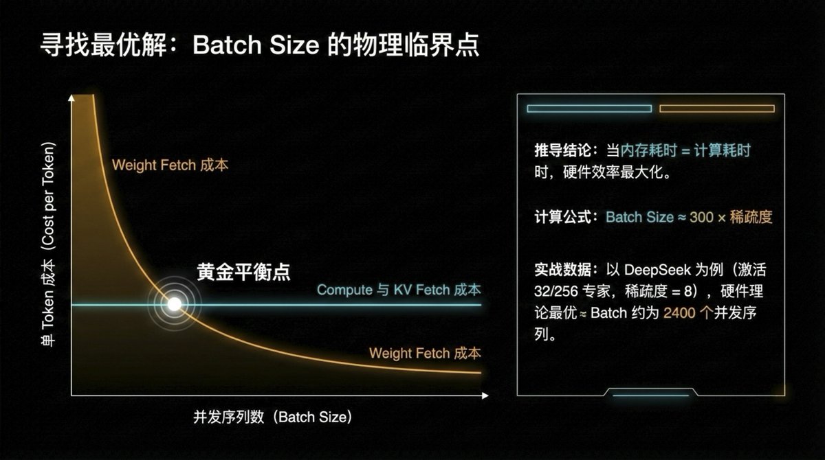
是什么卡住了模型的上下文长度?不是计算,而是内存带宽瓶颈!Dwarkesh 最新播客首次启用的黑板讲座 - 嘉宾Reiner Pope 曾在 Google 负责 TPU 架构,现在创立了芯片初创公司 Maddox,他用数学推导解释了 LLM 推理和训练的底层经济学👀
推理一个 token 需要的时长取决于“计算与内存时间“这两个瓶颈中更慢的那个:实际推理时间 = max(T_compute, T_memory)。
在小 batch size 时,内存带宽是瓶颈(要加载全部权重但只服务一个用户);在大 batch size 时,计算成为瓶颈。两者相等的交叉点就是最优 batch size。
计算成本随上下文长度几乎不变(因为注意力的计算量相对权重矩阵乘法很小);但内存带宽成本随上下文长度线性增长(需要加载 KV cache)。
稀疏注意力可以帮助(DeepSeek 论文中是平方根改善),但不是无限的——太稀疏会损失质量。
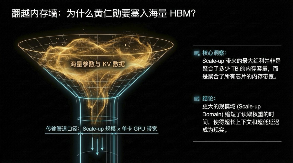
"我实际上看不到解决内存墙的好路径。HBM 就是现在这个水平,不会大幅改善。"
这直接回应了 Dario Amodei 的观点("不需要持续学习,in-context learning 就够了")——如果你需要等同于"与你工作一个月的同事"的 context,那可能需要 1 亿 token 的上下文窗口,在现有内存架构下成本极高。
内存(HBM)是真正的瓶颈!Pope 的分析从第一性原理证明了 Dylan Patel 反复强调的"DRAM 还要翻 2-3 倍"。内存带宽决定了上下文长度上限、推理成本下界、最优 batch size。SK Hynix、三星、Micron 是直接受益者⚡️

中文
Mr. Vinyl 美股投资之路 retweetledi

@Balder13946731 暴露出,大众,对AI价值链的浅薄理解。真稀缺的,从不是算力,是带宽。AI早撞上MemoryWall。。GPU算力再强,数据喂不进去也白搭。HBM是破这墙的关键。TSV硅通孔 + 多层DRAM垂直堆叠(8-16层甚至更高) + 逻辑基底die + 2.5D先进封装,实现单GPU数TB/s的超高带宽和极低延迟。大韩拿捏AI的命脉🇰🇷🫡
中文
Mr. Vinyl 美股投资之路 retweetledi
上文已经让大家了解了光通讯的产业链构成,那我们今天来讨论一下备受关注 $LITE $COHR $MRVL $CRDO 在这个产业链里处于什么位置?我们在交易的到底是什么预期?
提示🔔本条最好结合上一条一起服用。理解加倍~
本文内容很干,建议收藏随时复习
——————————————
$LITE 和 $COHR 占据中间三个核心位置: 外延/芯片;激光器,光模块。
$MRVL 和 $CRDO 占据后段两个环节,光模块和交换机。
$AVGO 除了光模块和交换机之外,少量生产激光器。
——————————————
LITE vs COHR — 激光器/光模块层的两强
$LITE 目前技术领先, 核心护城河是 EML 芯片。200G/lane EML 全球唯一量产,1.6T 光模块的不可替代光源,NVIDIA 直接投资 20 亿美元锁定产能。商业模式偏"卖芯片"而非整机,毛利更高。
但是体量小、产能跟不上需求。尽管产能已提升约 40%。 但还是"有单不能全接"。
但也说明一旦 Coherent 或其他竞争者的 200G EML 工艺成熟,需求端的溢出订单会快速被分流。不过这个验证过程通常需要2-3年。
主要客户:NVIDIA、各大云厂商光模块集成商。
$COHR 是这两个板块规模最大的玩家,占全球光模块市场份额约 25%,FY2025 营收 58 亿美元,是 LITE 的三倍多。
它的优势是全链条整合——从外延芯片到完整光模块一条龙,客户黏性强。
劣势是在最关键的 200G EML 这个技术节点上落后 ,当前仍是 100G EML 的主力供应商,追赶需要时间。
主要客户:微软、谷歌、Meta、亚马逊等超大规模云厂商直接采购。
不过两者在 CPO 时代都是 NVIDIA/Broadcom 的指定合作伙伴,不是零和竞争。
——————————————
AVGO 光模块和交换层的王者
$AVGO 博通是这条链里地位最高的玩家。
因为它既做交换 ASIC(Tomahawk 系列)又做硅光 PIC,是整个 CPO 生态的平台定义者——它的规格就是标准本身。
Tomahawk 5 Bailly 是全球首批量产 CPO 交换机,已出货 5 万台以上。
劣势是体量太大、增长弹性相对有限,且战略上两条腿走路(既做 Pluggable ,又推 CPO),有内部利益冲突。
主要客户:所有超大规模云厂商,几乎没有人能绕开它的交换 ASIC。
————————————————
MRVL vs CRDO 光模块和交换机的角逐
因为博通的🫅地位无法撼动,但是蛋糕太大,增长太快,所以 $MRVL 和 $CRDO 也获得了令人瞩目的增长。
$MRVL 专注定制化的芯片设计
定制 ASIC 和硅光 PIC都做。高度定制化是他拿下谷歌 TPU、亚马逊 Trainium 的网络芯片的最重要原因。
劣势是左右互搏。Pluggeble受益,但CPO就...
它是最大的光模块 DSP 芯片供应商,但 CPO 恰好会消灭 DSP 这个环节,所以它花 55 亿美元买 Celestial AI 来对冲。目前处于战略转型的阵痛期。
主要客户:谷歌、亚马逊、微软。
$CRDO 是三者里最小、最聚焦也最激进的一个。
它发明了 AEC 主动电缆,凭借这个产品吃到了 AI 建设浪潮的大红利。在 scale-out 以太网短距铜缆互联这个细分赛道几乎没有对手。
起初光通讯的普及对他的业务会产生致命冲击,所以它即使转型,在 今年 4 月花 7.5 亿买 DustPhotonics 强行切入硅光 PIC,转型初期风险较大。不过如果这一战略成功,那它“光电双收”。
——————————————————

Fiona ❤️& ✌️@nft_hu
如果你想真的了解光通讯产业链,那以下的内容不容错过——一图了解全产业链。 文章稍长,但是把光通讯的每个环节都讲的清楚明白需要费一些笔墨。 光通讯相比较电信号本质上还是一种信息传输的方式。只是光通讯更加高效,可以传递的信息量/速度都远优于传统的电缆。现在数据中心不可逆的趋势,就是需要传递的数据量的指数级增长。这个背景下,光通讯的流行和应用是势之必然。 —--------------------------- 整条链我分成了6个板块,我们一个一个来看。 1️⃣原材料,基本中国是龙头 铟(Indium)是一种稀有金属,主要产在中国,全球产量里中国占60%以上。铟本身没什么特别用处,但和磷结合之后,就变成了磷化铟(InP)——这个组合有一个神奇的物理特性:通电之后会发出激光。 镓(Gallium)也是稀有金属,中国2023年宣布出口限制,和砷结合变成砷化镓(GaAs),也能发光,用在短距离的场景。 做一个类比:原材料就像是"面粉"。面粉本身不是食物,但没有面粉就做不出面包。铟和镓就是制造激光器的"面粉"。 2️⃣衬底层 把铟和磷在极高温度下熔融、结晶、切片,就得到一片圆形的薄晶圆,叫做磷化铟衬底(InP Substrate)。直径约4-6英寸,看起来就像一片黑色的圆玻璃。 它是所有后续加工的基础材料,就像做芯片要先有硅晶圆一样。没有这片衬底,后面的激光器根本没有东西可以"长"在上面。 衬底就是"白纸"。在上面可以画出激光器的电路结构。 $AXTI 是全球最大的白纸供应商,占全球60-70%的份额。另一家是日本住友。 3️⃣外延/芯片 拿到InP衬底之后,用一种叫外延生长(Epitaxy)的技术,在这片晶圆上一层一层地沉积几纳米厚的半导体薄膜,形成精密的量子结构。这个过程就像在白纸上精密印刷电路。 这步做完之后,晶圆上就有了激光器的"基因"——一个可以在通电后发光的微小结构。然后把晶圆切成一个个极小的芯片颗粒,每一颗就是一个激光芯片(Laser Die)。 外延相当于"在面团上发酵",让基础材料产生功能性结构。这一步技术门槛极高,良率只有15-50%,大量芯片在这步就报废了。 4️⃣激光器——让“信号”发光 激光器就是把上一步做好的激光芯片封装成一个可以使用的元件。通电之后,它会发出特定波长的红外激光——肉眼看不见,但光纤最爱传这个波段。 激光器是灯泡,光模块是台灯。没有灯泡,台灯就是一个空壳。 5️⃣光模块——光电世界里的翻译官 光模块(Optical Transceiver)是一个大约手指大小的小盒子,直接插进服务器或交换机的插槽里。它里面装着:激光器(发光)、光探测器(接收光)、驱动芯片、镜头和光纤接口。 它的作用是双向翻译:服务器发出电信号 → 光模块把它变成光信号打进光纤;光纤传来光信号 → 光模块把它变回电信号送给服务器。 光模块是连接两个世界的翻译官,他把光世界的语言和电世界的语言来回翻译。 6️⃣交换机层 ——指挥交通、分拣信息 交换机(Switch)是一台专门负责"分发数据"的设备,长得像一个扁平的大铁箱子,正面插满了几十上百个光模块插槽。 在AI数据中心里,成千上万台GPU服务器要互相通信——比如一个大模型训练任务,可能同时用到1万块GPU,它们之间每时每刻都在交换中间计算结果。交换机就是负责把这些数据包准确、快速地送到对的GPU。 一台顶级AI交换机(比如博通的Tomahawk系列)上面可以插128个800G光模块,每秒总吞吐量超过100Tb。 交换机很像我们现实世界的快递中转站。每个包裹(数据包)进来,它看一眼地址,立刻分拣到正确的出口。速度极快,几纳秒就完成一次分拣。 —--------------------------- 最后的最后,就是大客户们买单了。 看完这这链条,再炒CPO光通讯,心里是不是有谱多了?
中文
Mr. Vinyl 美股投资之路 retweetledi

市场都知道四巨头烧钱,但有没有想过一个问题:接近 7000 亿美元的 AI 资本开支,最后到底便宜了谁?
整理了5个方向:
1.能源基建:算力的尽头是电力,更是输配电。
非常卡脖子的是输配电设备:变压器、开关设备、微电网。
一个吉瓦级的数据中心,对变压器和电网连接的升级需求是成倍的,目前北美高压变压器的交货周期已经长达两三年。
2.ASIC 设计与 IP 服务
亚马逊的自研芯片年化收入突破了200亿,谷歌也有TPU,说明大厂自研ASIC的替代已成气候。
大厂缺乏底层物理层的设计能力,这就需要博通和Marvell以及Arm这样的芯片定制设计服务商
3.存储
市场对 HBM的炒作非常充分了,但很容易忽略eSSD,企业级固态硬盘。
本地算力中心对庞大参数的存储,会疯狂消耗16TB 甚至 64TB 这样的大容量eSSD
4. 网络层:光电共进,光模块,铜缆
短距离互连上,高速铜缆还在爆发。
5.先进封装设备与测试
台积电的产能瓶颈在 CoWoS 这样的先进封装产能。
能提供先进封装所需的贴片设备、热压键合设备、混合键合设备的供应商是卡脖子环节。
随着芯片越来越复杂,为了保证良率,半导体自动化测试设备的使用量和测试时间都在大幅增加,这也是一个量价齐升的隐蔽环节。
这五把铲子,都会是承接这7000亿美元泼天富贵的受益者。
Terry@RichTerry123
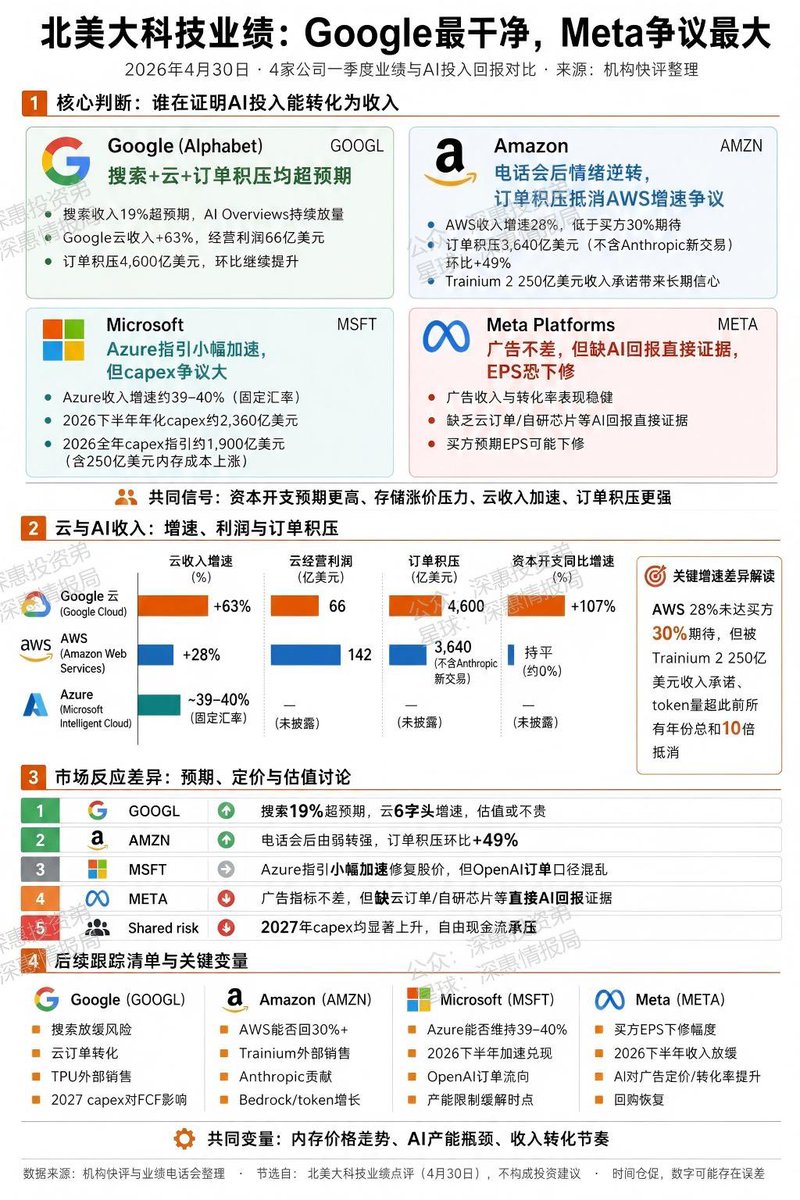
昨晚的四巨头财报总结了一下: $GOOGL Cloud 增长 63%,Pichai 说收入本可以更高,只是受算力约束。 $MSFT Azure 重回 40% 增速,Copilot 付费席位继续增加。 $AMZN AWS 增长 28%,自研芯片年化收入突破 200 亿美元。 $META 广告变现已经验证,但 AI 独立变现还是比较模糊的。 Pichai 说算力供给跟不上需求,微软管理层Nadella 说 Azure 需求比产能增长还快。 这些话从产业最前线说出来,比任何分析师报告都更有说服力,现在的算力是供不应求的 谁能拿到更多的算力芯片、谁能搞定更多的数据中心能源配额,比如OpenAI在AWS锁定的2吉瓦算力,谁就能吃下更多的市场份额。 算力即权力的逻辑在2026年依然坚不可摧。 芯片、HBM、光互连、电力、液冷、数据中心设备,仍然是最硬的主线。
中文
Mr. Vinyl 美股投资之路 retweetledi
